I would like to know what kind of output comes from the trigger input to FPGA pin on Open ADC when I give input to LNA. Is the trigger input to FPGA ‘1’, the moment ADC output is available at ADC0… ADC9? If so, how long does it stay high? Does it happen at every clock cycle?. What’s the relationship between LNA input, ADC clock, trigger input to FPGA and the ADC outputs. The reason I’m asking these questions is because I would like to know if I need to design any other logic on the FPGA end. Could I just straight away connect the trigger signal as an input signal? And if the trigger input is ‘1’, then could I store the ADC data from ADC0… ADC9 bits onto the FPGA memory?
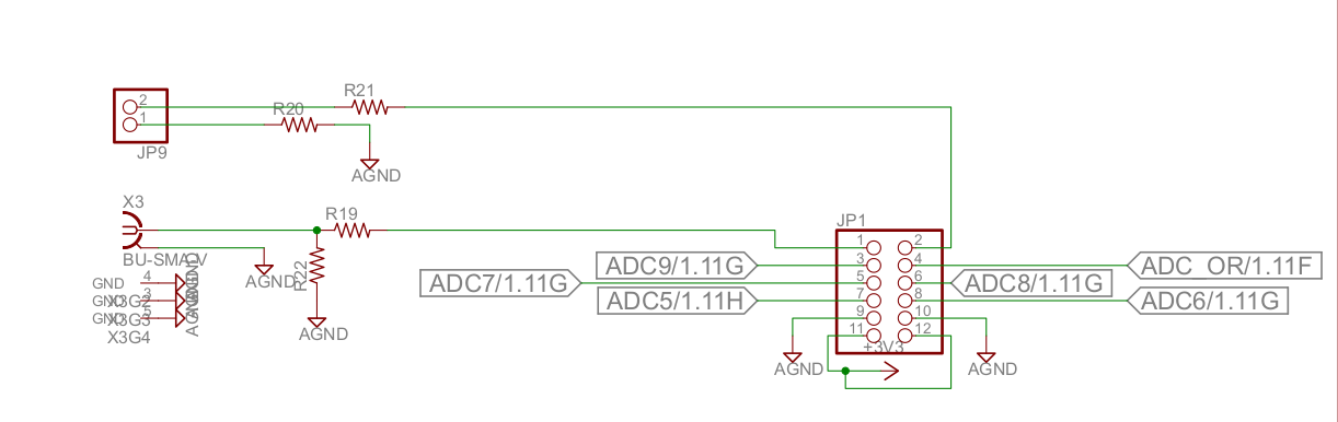
From the schematics (in the link you sent) but also from the original ones I found bellow pin 2 is simply connected to JP9 hence I think it does not do much.
Okay. Thanks, ExMachina. So, only if I give a trigger signal at JP9, would it generate a trigger input signal to the FPGA.
Do you have any idea on how long I need to hold the trigger input signal high for? Are there any recommendations?
In such a setup the real trigger logic is inside the FPGA fabric so depends on your code inside the FPGA. I think it is safe to say that the signal should be valid for at least a clock cycle.
In the chipwhisperer code for example the triggers can be found here … somewhere
Trigger configuration