Glitching on third party board

Hi everyone,

I met a comprehension problem after reading third party glitch. Indeed, I talk about Hardware Setup section.

What I don’t well understand at first, it’s the purpose of the 7th step (" 1. Add a header pin/wire to RST (First column from the left, third row from the bottom). The CW-Lite needs two connection points, as we’ll be both resetting this pin and triggering off of it.")
because in the wiki glitch tutorial, Pin-16 of the CW-Lite is used for trigger input and because the “trigger_high()” function set the GPIO at high level to trigger it.

So, why the pin-16 of the CW-Lite is connected to the NRST ? Is it specific to the bootloader attack application ?

Then, my other question is about the 6th point of this same topic. I compare the hardware setup with the R3 (12-ohm resistor) between STM32F3 target board provided by New AE Technology and the target board of the tutorial. In the tutorial, it’s explained to “Add a 12-ohm resistor on the 3.3V_CORE jumper” but when the SMA connector is connected to VCC, the glitch output will be automatically connected to the R3 resistor.

And so, by comparing with the following schematic, we don’t have “SHUNTL” after R3 resistor and “SHUNTH” before R3 resistor ?

image|690x418

Théophile

Hi Theophile,

For that tutorial, we were attacking a microcontroller’s built in ROM bootloader. For this target, like most realistic setups, we don’t have a GPIO pin that gets set high before the operation we’re interested, so we have to find another way to trigger the glitch. In this case, we’re using the reset pin, as the operation we’re interested in bypassing, the fuse read, occurs after the device is reset.

For your second question, I believe the terminology is just a little ambiguous here, as there’s not typically a distinction between a microcontroller’s VCC and the general board VCC. It’s the same setup for both - connecting the glitch to the low side of the shunt resistor.

If you look at the picture that follows the procedure for modifying the board, you can see that the blue wire that connects the SMA connector to power goes directly to the microcontroller’s power pin:

Hope that

Hi Alex,

There’s still something I don’t understand about the third party setup as we can see in the tutorial. In fact, what’s the purpose of the R3 resistor (or 12-ohm resistor) ? By the way, why 12-ohm resistor ?

In fact, I don’t even understand the position of R3…

Hereafter, I made a schema to show you what I understand by considering your explanations and the tutorial explanations…

Theophile

Hi Theophile,

R3 mostly just makes it easier to drop Vcc-in to ground. The resistor being 12 ohms isn’t really anything special, it’s just a reasonable value. For example, 100 ohms would likely drop too much voltage for the microcontroller to run properly and 0.1 ohms wouldn’t really do much.

Alex

Hi Alex,

I still meet some problems in my purpose of glitching a third party board.

The first thing I don’t manage to understand is about the interconnexion.
Indeed, I compare interconnexion from the glitching_third_party example and the interconnexion with the provided STM32 target board (connected to CW308 UFO BaseBoard).

Below the screenshot of the provided STM32 target board (connected to CW308 UFO BaseBoard).

In this screenshot, SHUNTH is connected on the high side of R3 = 12 Ohm resistor and SHUNTL is connected on the low side of R3 = 12 Ohm resistor. From this screenshot, where the voltage (in normal mode) come from ? then, where the voltage (in glitch mode) come from ?

Furthermore, to make a link with the code coming from Jupyter Notebook when we use
scope.io.glitch_hp = True, does this mean we will use the SHUNTH way to perform glitch ? then, same with scope.io.glitch_lp = True and SHUNTL ?

I missed explaining my second question in my previous message…

I well understand the R3 value but I don’t understand the R3=12ohms position from the available example glitching_third_party.

In fact, what is special in this example, is that there is only the center pin (SHUNTL) connected to Vcc but the third pin (SHUNTH) isn’t connected to the high side of the 12-Ohm resistor-> Why ?

In my case, here is Vcc input :

As STM32FX target board provided by New AE Technology, I have a VCAP1 and VCAP2 with decoupling capacitors. I imagine that if I want to glitch my third party thanks to this Vcc input, I will have to cut C13 and C12, then connect M10 and F13. But after all of that, can you explicitly explain me the thing I have to do to connect the SMA connector please ?

Furthermore, It seems that a BYPASS-REG way exists (supply my board without regulator control). Can you another time explicitly explain me the thing I have to do to connect the SMA connector please ?

Thank you by advance !

Théophile

Hi Theophile,

The power always comes from the CW308, which itself is either supplied by the ChipWhisperer, or via the DC barrel jack, into FILTIN and out of FILT_LP/FILT_HP, where they connect to SHUNTHP. There is no difference when you’re running normally or when glitching - all the glitch is a MOSFET that shorts SHUNTL to GND.

The voltage is always pulled low on SHUNTL. glitch_hp and glitch_lp are two separate MOSFETs on the ChipWhisperer-Lite. The LP MOSFET operates more quickly, but can’t handle as much current as the HP MOSFET.

In your case, it looks like it would be best to try replicating what we do on the F2/F4 and bypass the STM’s internal voltage regulator. There, we feed a voltage directly into VCAP1/VCAP2, which are the output of the internal voltage regulator, which is higher than the typical output voltage (we use 1.2V for the F2/F4, which works fine in most cases). This keeps in the internal regulator off.

Yup, that’s correct.

As for connecting the SMA, you’ve got the right idea in your post from July 29. Does this schematic show things clearly (CW 1.2V is coming from the 1.2V supply on the CW308 board):

image

I’m not sure what BYPASS-REG is in your diagram. Do you know what device U6B is? I’d like to check the datasheet for it if available.

Typically what I described above is enough to bypass an internal regulator, but there might be additional complications here.

Alex

Hi Alex,

Thanks to your response !

As for connecting the SMA, you’ve got the right idea in your post from July 29. Does this schematic show things clearly (CW 1.2V is coming from the 1.2V supply on the CW308 board):

In my case, I don’t want to use CW308 even more. So what it implies about the schematic you shared ? Because from the CW-Lite, we just have a 3,3V supply.

I’m sorry but I don’t show you the well target from the schematic. The component I show you allows to control STLINK with a STM32F7 whereas in my case, I just want to attack a STM32U5.

Here is the schematic you asked me : https://www.st.com/content/ccc/resource/technical/layouts_and_diagrams/schematic_pack/group1/f1/6c/26/bc/a0/a0/48/d7/MB1549-U575ZIQ-C02_Schematic/files/MB1549-U575ZIQ-C02_Schematic.PDF/jcr:content/translations/en.MB1549-U575ZIQ-C02_Schematic.PDF

Theophile

What I’ve done, and found to be working, is removing the capacitor from the VCAP pin, and connecting the glitch output directly to the pin, without resistor. Did the trick in my case.

I was afraid of connecting an external voltage source to the pin, as the specs of the voltage regulator are too narrow and my own power supply is pretty noisy.

Thanks for the input!

@theophiledmt I’d say give this a shot, as this is simpler and avoids needing a 1.2V supply.

Alex

Hi Alex,

I don’t manage to see interconnexions without CW308 1,2V supply regarding the schematic you shared me in your second last post !

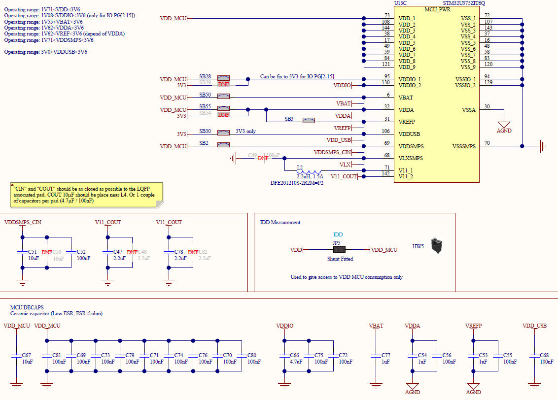
In my case, the target is a STM32U575 and his supply technology is based on SMPS… I don’t know if it could affect the glitch realization. From this diagram, what do you advise me to do to power the U575 and connect the SMA connector ?

Theophile

Check the datasheet if the power domain in the MCU is separated and uses different internal regulators for CPU, I/O logic, backup and so on. Most likely that will lead you to discard glitching on VBAT, VDDA and VDDIO.

I’d try looking into VDDSMPS and VDD11_x.

Continuing the discussion from Glitching on third party board:

Hi Schweik,

Thanks to your return !

Regarding the diagram below, it seems VDD11 skip the SMPS/LD0 internal.

Moreover, thanks to the datasheet :

VDDSMPS is the external power supply for the SMPS step down converter. It is provided externally through VDDSMPS supply pin and must be connected to the same supply than VDD.

In my case, if I connect 3,3V from CW-Lite to VCC_MCU, it will just supply the core or also the peripherals such as GPIO/NRST ?

Because, in my use case I need to supply at least NRST and another pin to trigger the glitch.

So, what I would have to choose ? Supply through VDD_MCU linked to VDD_x or VDD_MCU linked to VDDSMPS ?

Thanks for your help !

Theophile

Hi Alex,

I would have a last question about the reset of the target in case of glitching a third party.

In fact, from my glitching third party setup, I would like many things :

(1) Be able to reset the target (send a reset signal on the NRST pin of my target). If I’m not mistaken, on software side (from Jupyter Notebook), I just have to use “target.flush()”.

(2) Be able to know when the target is in reset mode. I don’t know if the CW-Lite allows that because I understood that “glitch_loop” example from the tutorial plays on “scope.adc.timeout” to say if the target is in reset mode or not. Is it the case ?

Theophile

Hi Theophile,

You can toggle the nRST pin via scope.io.nrst = x where x is 1, 0, or None (high-z).

scope.adc.timeout is based entirely on the time between arming and not receiving a trigger signal. If you set the timeout to 2 seconds and more than 2 seconds pass between arming and receiving a trigger signal, then the scope times out. If this is sufficient for you to tell that the target is in reset mode, then you can use this to indicate if the target is in reset mode.

Alex

Hi @Schweik , @Alex_Dewar,

I performed the HW modifications but without glitch success.

What I made:

  • I remove decoupling capacitors on VCAP1/VCAP2 ;
  • I cut the trace between VCAP2 and the GND ;
  • I connected directly the SMA output on VCAP1 ;
  • I don’t connect any 1,2V with a serial resistor on VCAP1.

Here is the synthesis schematic:
image

According to you, is it mandatory to interconnect VCAP1 to VCAP2 before connecting it to SMA output ?

I made some measurement with an external scope and I could see that no one shunt is performing. @Schweik you said that I worked in your case but did you keep a minimum low voltage ( < 1,4 Volt on the VCAP trace) ? because without it, I don’t understand how you can put down voltage.

Thanks by advance to your return

@theophiledmt In my setup the VCAP was output of internal voltage regulator. I’m not too familiar with that particular STM MCU, but it appears the case is the same, and in addition the MCU can be configured for using an external supply on these pins in software.

If these pins are output of a voltage regulator, shorting them to ground (with CW, not manually) should work. Attach a scope to the SMA connector - is there any voltage there? What happens when the CW outputs a glitch?

Also, does that MCU have two power domains?

@Schweik I made the same setup as your and it allows me to glitch the loop example provided by NewAE. But for more stability, I preferred supplying the VCAP1/VCAP2 input with 1,2V from the CW308 UFO board and a low resistor (~16 ohms).

1 Like