Hi, I’m trying to voltage glitch an Stm32f103 to gain access to the flash memory and dump the firmware. I’m basing my thinking on this glitch paper https://www.google.com/url?sa=t&source=web&rct=j&url=https://tches.iacr.org/index.php/TCHES/article/download/7390/6562/&ved=2ahUKEwi087W0p8DnAhV30TgGHVQ8BPkQFjABegQIBRAM&usg=AOvVaw3Yf850otJLHvHHJiRQLcVi
Anyway I somehow have to coordinate the read Flash command via openocd and stlink v2 adaprer and use it as a trigger for the chip whisperer lite. Does anybody have any ideas on how I might go about this or if there is an easier way to gain flash access.
Hi,
Ideally you would have an FPGA to passively observe the JTAG traffic and issue a trigger to your ChipWhisperer at or around the “right time”.
But all you really need is a constant time reference that you can use to time your glitch, since you can offset and sweep from there with the ChipWhisperer. I’m not sure what’s the simplest way to do that, I’m just pointing you in (hopefully) the right direction.
One option is to adapt our PhyWhisperer-USB for your purposes, as explained here.
You might also get some ideas from Dmitry’s bootloader bypass tutorial.
Jean-Pierre
OK so your suggesting to use a phy whisperer USB hooked up to my stlink v2. Sniff the USB line of the stlink and wait for the read Flash message and use it as a trigger for chip whisperer?
That might work but I don’t know whether the USB traffic can serve as a constant time reference?
Ideally you’d customize the PhyWhisperer FPGA to sniff the JTAG itself. It’s got a bank of 8 I/Os that were put there for these kinds of situations. But it does require you to customize the FPGA bitfile yourself.
Jean-Pierre
Hello, fridgyylife
I has sucessful break crp level 1 on STM32F103 and script this here
Best reguad,
Nik.
3 Likes
Hello I’m looking for to described metod for gain access to the flash memory at Stm32f103 . Do you can that now? Could you send me how to do that? Thanks.
I am trying to do the “same” attack on my stm32f2 (set to rdp1) chip only that I attack the bootloader read mem cmd (0x11). (Like this Russian dud in the link above)
By sending the read command 0x11, 0xEE and then glitch just before I get the respond (nack) I from time to time hit the correct location where rdp is checked and I get an ack.
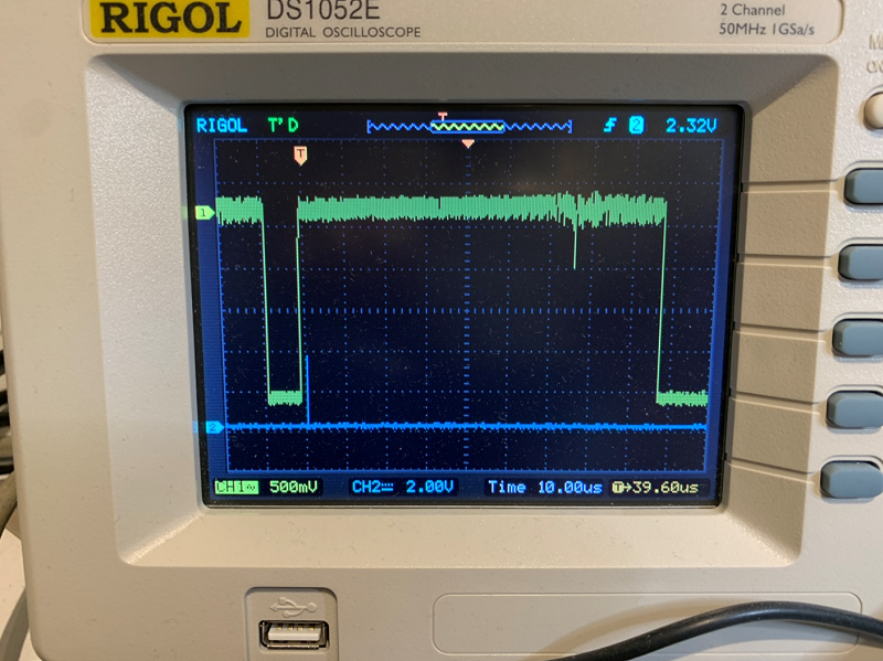
I have set my trigger to tio2 (serial tx) and I arm the scope after sending 0x11 but before sending 0xEE.
My problem is that the time used to sending the byte 0xEE is not constant and after sending all bits I see my trigger point is off by 100 to 1000 clock cycles (clock @ 96mhz)
From time to time (like after 50 to 100k glitches) I hit something that trigger a chip erase etc and after this I read only 0x00 bytes from the lower part of the chip flash.
Does anyone know how I can set the trigger on the last bit transmitted over serial instead of the first bit so that I get a more accurate trigger point? (Or perhaps there is a better way to trigger?)
Atm my offset is ~14000 clocks at 57600 bps serial speed (8E1) and if I could trigger the last bit I might reduce this offset to like ~1400 ish. I believe that the trigger could be a bit more accurate if I could do this.
It would be pretty tough to do that with the Lite, but the Pro does have an actual UART trigger. The same thing can be accomplished by using the trigger output of an oscilloscope if it has a UART trigger as well.
That was one fast respond 
So I guess there is no way to have like a trigger counter and after arm then trigger when trigger counter is equal to 10 ish?
I do believe there is such a counter in there some place?
There is a cycle counter between ADC trigger events (that’s scope.adc.trig_count), but not a trigger counter itself. Your idea I think would be possible, but would require modifying the FPGA code.
I am pretty new to this so for me to mod the FPGA is probably not the best idea
But perhaps this is something that others also could use and could be a nice feature for an upcoming update?
Btw. Will the FPGA be updated automatically when I pull new updates from git or do I have to manually update it?
Anyway. That idea using the scope / something else as a trigger was a good one.
I can use some external STM/Nucleo chip set up with an interrupt on a pin and let it could the bits transmitted over serial for so to trigger the CW when last bit is to be transmitter.
Thank you for your help
The FPGA gets reprogrammed every time you power cycle + connect, so as long as you’re on the latest software update, you should have the latest FPGA code. I believe we have updates/fixes for the FPGA somewhere (probably far away) in the pipeline, so we’ll keep this in mind when we take a look at that .
I have implemented CAN bus support and this is much more stable now that I can control the external clock. I run the hs2 at 24MHz and by counting the number of rising edges I see in the CAN msg I send I am able to set a trigger on the last edge just before CAN EOF (7 recessive bit) is sent. (Coz of bit stuffing I calc this number at runtime)
This will trigger the CW to glitch with an offset of 1560 clock cycles and my range is from 1560 -> 1562. This is way more stable compared to using serial.
But now since I run the clock at 24 Mhz I loos a bit of resolution and I would think that if I could run the glitcher at 96Mhz and the hs2 at 24Mhz I would get an even better glitch offset.
The reason for this is that from one chip to another I see that going from 1560 to 1561 is to fare and the result is only zero when I read a block (256 bytes).
I can get around this by adding a nop or two just before I trigger CW but I think if I could run the glitcher at 96Mhz I could drop these nops.
Q1) Is it possible to set the internal clock on the CW to say 96Mhz and still be able to use hs2 to clock the STM chip at 24MHz?
I have had great success with both “glitch_only” and “enable_only” but the last one was better when running at 96 MHz using a repeat of 3. This is a bit smaller I think compared to repeat 1 at 24Mhz. Using the “glitch_only” I can set a smaller width and a bit different offset if I understand this correctly but I am still a bit confused about the negative width and offset.
Lets say a the start of a clock is when the edge is rising and the middle is where it goes down and the end is where the next clock start (rising again)
Q2) Will offset -50 be at the start? And offset 0 in the middle? And offset +50 at the end?
If so then say I have a offset of -40 then how can I have a negative width? Will a with of -10 in this case be the same as using offset -50 and a width of +10 (Just like a negative width goes backwards in time)?
-
I think you could generate the clock externally and feed it into both the STM and the ChipWhisperer, which would allow you to use the CW’s clkgen to generate whatever clock you wanted.
-
The enable signal for the glitch will start on the falling edge of the delayed glitch clock. This diagram might make things a little clearer:
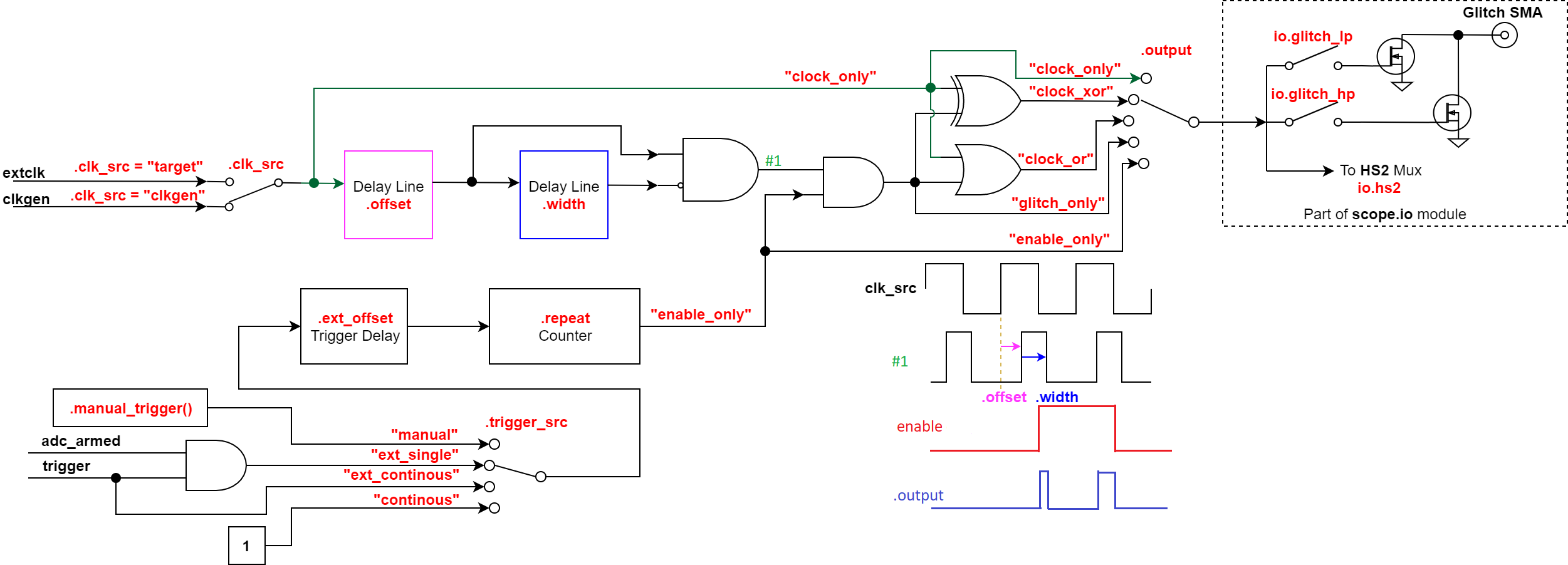
Though move the rising edge of the enable signal to the falling edge of #1 due to recent changes.
Alex
Nik,
Where can I get the jupyter notebook that you used for this?
Hello,
Could someone explain exactly where to put the glitch?
0x11 - 0xEE - ACK
Is it after 0x11 shifted out but 0xEE not started yet?
Or is it during 0xEE?
Or is it after 0xEE and before ACK received?
Also with some timing that worked for you.
Thank you!
Hi, I know this is quite late but would you happen to have the notebook available for download?
Thanks,
Nick
Did you ever manage to get it more stable and not erase itself while dumping? I am currently trying to read out some firmware and I am slowly but surely descending into a black pit of despair because no matter what I do, the chip erases itself after a handful of successful glitches all the time.
I can also see a some jitter between the CAN message arriving at the target and the response that is sent out. I suspect that this is the reason I am occasionally hitting the wrong spot that triggers the chip erase. I just fear that this isn’t something I can prevent.
My glitcher is pretty stable now and I can read out a lot of 256 bytes block before I hit a chip erase. (My targets are the STM32F2 and STM32F4 where the F4 needed even more stable glitches)
I use CAN only (USART is way to unstable) and just after I send a CAN msg I power cycle the chip for so to try again. If a chip erase is triggered then only the first sector is erased and this is why I dump this sector 2-3 times before I continue. (from time to time I get the wrong data on these addresses)
Using this approach I can see that the first sector is erased but the rest of the chip’s content is intact. Dumping the F4 1meg version takes like ~20hrs and only the first sector will be erased.
So not the best solution but it “works”. And yes. I believe I could be unlucky and hit an erase before finishing the first sector but that have never happened to me yet
I ordered a lot of chips from AliExpress coz I could see that many of these “brand new” chips came with RDP1 set. I could then dump these chips and see the original content…
Hop this helps.