I tried to generate a bitstream from source for the CW-lite Xilinx project (Auto generated using your script)
It synthesises but I get the errors during the ‘map’ process.
I am sure that I shouldn’t be seeing this . Do you know what I am doing wrong?
Thanks in advance!
[code]ERROR:Place:1205 - This design contains a global buffer instance,
<reg_chipwhisperer/clkgenfx_mux>, driving the net,
<reg_chipwhisperer/rearclk>, that is driving the following (first 30)
non-clock load pins off chip.
< PIN: target_hs2.O; >
This design practice, in Spartan-6, can lead to an unroutable situation due
to limitations in the global routing. If the design does route there may be
excessive delay or skew on this net. It is recommended to use a Clock
Forwarding technique to create a reliable and repeatable low skew solution:
instantiate an ODDR2 component; tie the .D0 pin to Logic1; tie the .D1 pin to
Logic0; tie the clock net to be forwarded to .C0; tie the inverted clock to
.C1. If you wish to override this recommendation, you may use the
CLOCK_DEDICATED_ROUTE constraint (given below) in the .ucf file to demote
this message to a WARNING and allow your design to continue. Although the net
may still not route, you will be able to analyze the failure in FPGA_Editor.
< PIN “reg_chipwhisperer/clkgenfx_mux.O” CLOCK_DEDICATED_ROUTE = FALSE; >
ERROR:Place:1136 - This design contains a global buffer instance,
<reg_chipwhisperer/clkgenfx_mux>, driving the net,
<reg_chipwhisperer/rearclk>, that is driving the following (first 30)
non-clock load pins.
< PIN: target_hs2.O; >
This is not a recommended design practice in Spartan-6 due to limitations in
the global routing that may cause excessive delay, skew or unroutable
situations. It is recommended to only use a BUFG resource to drive clock
loads. If you wish to override this recommendation, you may use the
CLOCK_DEDICATED_ROUTE constraint (given below) in the .ucf file to demote
this message to a WARNING and allow your design to continue.
< PIN “reg_chipwhisperer/clkgenfx_mux.O” CLOCK_DEDICATED_ROUTE = FALSE; >
ERROR:Place:1136 - This design contains a global buffer instance,
<reg_clockglitch/gc/dcm1_clk_out_BUFG>, driving the net,
<reg_clockglitch/gc/dcm1_clk_out_BUFG>, that is driving the following (first
30) non-clock load pins.
< PIN: reg_clockglitch/gc/Mmux_glitched_clk1_SW0.A5; >
This is not a recommended design practice in Spartan-6 due to limitations in
the global routing that may cause excessive delay, skew or unroutable
situations. It is recommended to only use a BUFG resource to drive clock
loads. If you wish to override this recommendation, you may use the
CLOCK_DEDICATED_ROUTE constraint (given below) in the .ucf file to demote
this message to a WARNING and allow your design to continue.
< PIN “reg_clockglitch/gc/dcm1_clk_out_BUFG.O” CLOCK_DEDICATED_ROUTE = FALSE;
ERROR:Pack:1654 - The timing-driven placement phase encountered an error.
[/code]
Sorry on the delay again… apparently my e-mail-me-on-posts stopped working
Basically you just have to put those constraints in the UCF file, I might not have committed them for some reason (i.e. the one that says “PIN “reg_clockglitch/gc/dcm1_clk_out_BUFG.O” CLOCK_DEDICATED_ROUTE = FALSE;”).
These come up as I’m forced to do some “non-nice” things in the FPGA to generate the clock glitches… the FPGA tools don’t like one purposely generating glitches, so for example I’ve got to route clocks onto the FPGA fabric to XOR them together, then route them out pins.
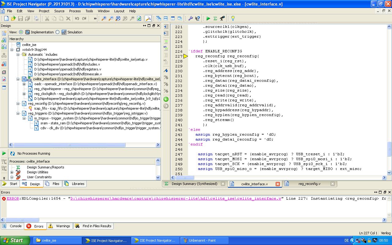
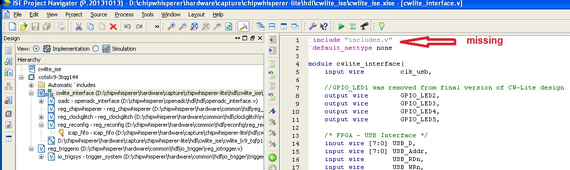
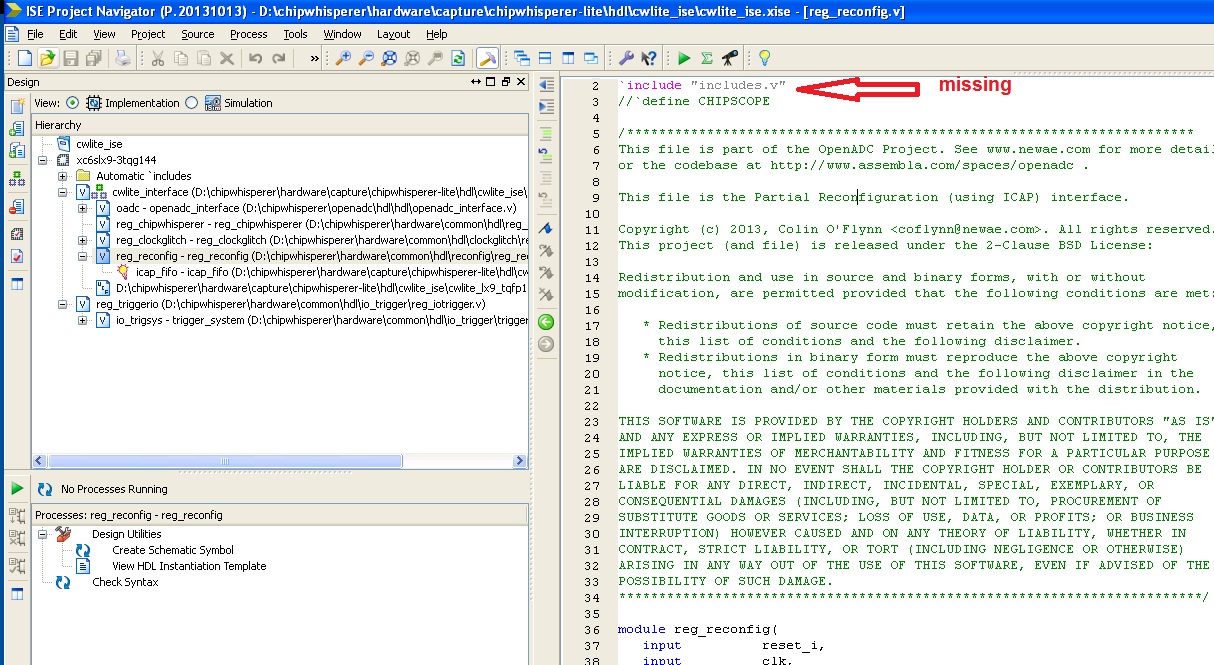
Thanks Colin, it was my bad . My .ucf file was somehow under the hierarchy of the reg_reconfig module instead of the top level module (cwlite_interface).
I am having another error ; probably again a very silly issue … Any advice on how to go about solving it? Sorry I am a terrible newbie at FPGAs
Place:1355 - Component < N48 > is driven by DCM or PLL component < reg_clockglitch/gc/DCM_extclock_gen2 > placed at < DCM_X0Y0 >. This requires the load component to be range constrained to CLOCKREGION_X0Y0 or CLOCKREGION_X1Y0. Placer was not able to apply this range constraint because component < N48 > has a LOC constraint or area group in a different clock region. Please check whether the user constraints and remove any conflicting LOCs or area groups. Note that the loads of a DCM/PLL must be constrained to the two adjacent clock regions to the DCM/PLL. Using DCM/PLL clocks to drive clock pins directly is not a recommended practice. Using a BUFG will give more flexibility to the placer and produce superior placement results.
Ahh… that problem is not as trivial! I’ve got to check what settings I had to fiddle with - basically the device has some issues during placement, I had tried a while with locking down the location of everything without success. It’s rather annoying…
As a work-around for now (until I look up what I changed, should be able to do that today) if you’ve got time, try running the ‘SmartXplorer’, see xilinx.com/support/documenta … /ug689.pdf . This is basically a hack which tries multiple tweaked settings until one happens to work…
Great suggestion Colin!
SmartXplorer’s ‘Congestion Reduction’ option helped to generate several mappable options.
I was also planning to use CW-Lite with the Multi-Target Victim board but then, I realised that the Serial-Target module was not present in CW-Lite’s FPGA. Before I go about including that, it’d be nice to know if there was any reason / technical constraint causing it’s exclusion ?
Also, I checked that the LX25 FPGA used in CW-Lite has enough resources for us to double the ADC fifo size. It is nice to have a max sample size of 49k rather than 25k , with almost no effort
No “technical” reason… but my plan was to use the USART module in the SMA3U instead, which is much nicer than my FPGA UART module. However if you want backwards compatibility you can include it.
Yup - it can indeed! For some reason I started with a smaller buffer size and just kept that. Part of it was making it easier to meet timing, but the SmartXplorer can help with that.
My long-term plan was once the FPGA was more stable to try increasing the FIFO size, but I keep picking up all these other projects in the mean-time which delay me…
Today, I tried using the old reg_serialtarget.v module in cw-Lite and it seems somewhat unstable (works sometimes). Perhaps it’s due to the new clock speed.
So, i abandoned the old approach and tried to use the USART module of the SAM3U. It works nicely and I am now communicating with smartcards.


 . My .ucf file was somehow under the hierarchy of the reg_reconfig module instead of the top level module (cwlite_interface).
 It will work even better than the FPGA implementation…