Instead, if I set the output frequency to a lower value, like 20 MHz, then I just got the last warning (No nets matched ‘swclk_IBUF’). Also I don’t get timing violation.
If you want to replicate the bitstream generation, here’s the Github link with all the sources. The Vivado project is in the directory “CW305_DesignStart”.
I’ve uploaded the generated bitstream to CW305 in this notebook.
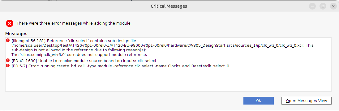
Hmm that first error is interesting. I’ve never come across this, and yet I’ve done this (generate a Vivado IP block and instantiate it in Verilog) so many times.
Looking at your Vivado project, this is where Vivado is trying to pull in the clock wizard block; is it the right path?
If you can resolve this, all the other errors should go away.
Hi, thanks for the reply.
I’ve changed the path to refer to the correct one, but I still have the same error. Is there some workaround?
You can check the updates still on the github link.
I’ve added a readme describing all the steps I’ve done.
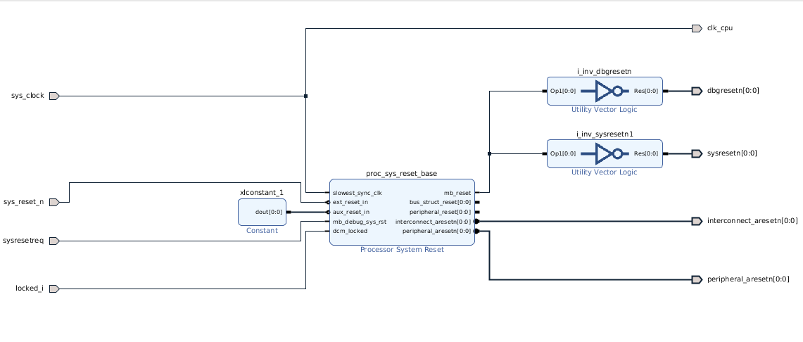
Also, how the block diagram of the clock_and_resets block should look like?
From the readme, mine looks the same as expected.
The clock_and_resets block diagram looks correct (the clk_select.v and clk_wiz_0 modules don’t reside there, despite their names).
I’m puzzled that you keep getting this error. There are reports about this problem on the Xilinx support forum, but I’ve never run into it myself (despite instantiating clock wizard blocks in pretty much all of my projects), and I haven’t been able to find a nice clean solution from those who have encountered this.
One option to avoid this issue altogether is to use this earlier version of our DesignStart recipe, prior to the addition of the clk_select module. Functionally, all you will lose is the ability to bypass the PLL, which only matters if you’re interested in clock glitching.
Looking around it seems that the problem is that the clock wizard does not support the XCI inferring.
A couple of forum topics talk about this (here and here).
I’ve tried some of the fixes suggested, but none of them worked. The only one I didn’t try was to use the IP packager to create a new IP from the clock wizard RTL files.
In the Vivado documentation, chapter 14 (XCI Inferencing) says that even if it cannot be added as an XCI, it should be at least possible to add it as an RTL module. But it didn’t work for me.
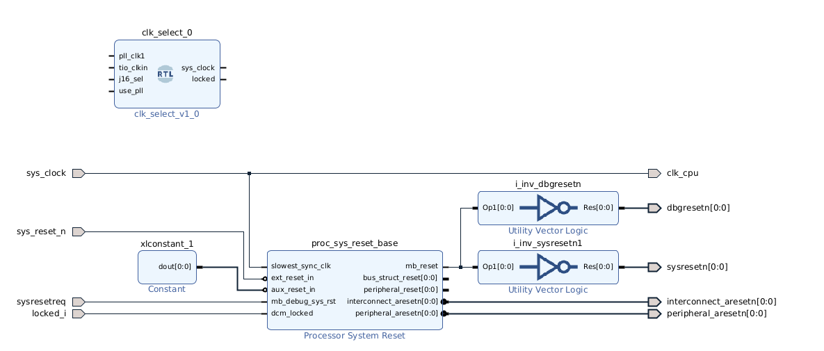
Anyway, with another version of Vivado (2023.2) I was able to add the clk_select_0 module in the clock_and_resets block diagram. I don’t know if the bug was due to the Vivado version or to the revision of the clk_wiz IP (upgraded from Rev.3 to Rev.13).
But, now I don’t know how to connect the clk_select_0->sys_clock to the sys_clock input pin.
Since I’m a novice in Vivado, surely I’ve been mis-interpreted some steps.
Here is the list of actions I’ve performed :
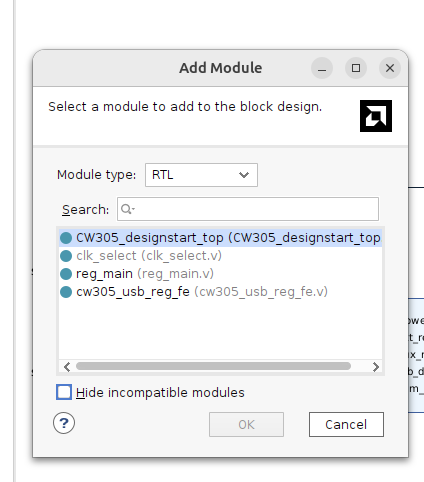
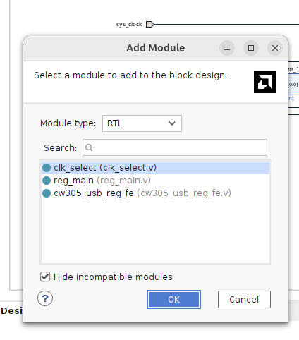
Following the readme I’ve tried to add the clk_select module, but since the source is added later on the readme, there was no module.
I’ve added the source files clk_select.v. When I tried to add the module it showed as incompatible
I created the clock wizard IP and then the clk_select module is shown as compatible. With Vivado 2019.1 I got the error, while with Vivado 2023.2 I can add it
I don’t know if it is the correct flow of operations. Do you see something wrong?
Also, If I added the clk_select module correctly how do I connect the clk_select_0->sys_clock to the sys_clock input pin?
But that’s not true - I know because I’ve done it! I’m quite puzzled why it’s not working for you; I’m sorry I don’t have a perfect solution, but the workaround I mentioned above (using an older version of our recipe) would avoid the issue entirely; as long as you don’t care about clock glitching, you won’t lose anything (and if you do care about clock glitching, then you can simply remove the clk_wiz block entirely; however I would still recommend that you start with our approach, to start with a known working point).
I also advise against using the newer Vivado version: when you get to the SW building steps, you won’t be able to follow along unless you use the version we prescribe.
Hi,
from what I understood the clk_wiz should support the XCI inferring. It’s just that my version of Vivado or the specific revision of the clk_wiz (mine is rev.3) that I’m using has some kind of bug.
What puzzles me though is whether I have followed the steps correctly.
I mean, even if I’m able to add the clk_select module, how am I supposed to connect the clk_select_0->sys_clock to the sys_clock pin?
Am I not trying to connect the output of a sub-module (clk_select) to the input port of the top-level module (clock_and_resets)?
Shouldn’t it be the other way around?
Indeed, Vivado doesn’t allow me to make this connection
Anyway, I’ll try to use the older version of CW305_DesignStart and I’ll keep you updated.
Thanks again for the reply
Hi,
I’ve been able to solve the problem with the clock not toggling.
The error was due to the frequency of the PLL.
I can’t understand why, but by setting the PLL with frequency lower than 15 MHz the soft core stays in the reset state. Maybe the PLL doesn’t work reliably with a frequency lower than 15 MHz.
Instead, with frequency higher the soft core works correctly.
You can check the notebook I’ve used here
Also, I’m using the older version of the CW305_DesignStart (as suggested ), since in my case the newest version doesn’t work (still the problem of not being able to infer the clk_select module ).
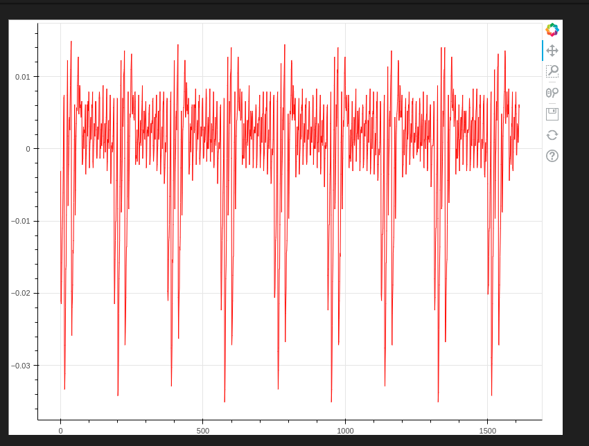
Capturing the power trace, this is what looks like :
Now I’m facing a new problem, I’m not able to communicate with the soft-core via UART since I’m using as scope the picoscope.
Can the USB connection be used to exchange data with the softcore?
Thanks again in advance
In general PLLs need to know what input clock frequency they’re getting in order to function properly. In this case it’s supposed to be 20 MHz.
Yes, all communication with the FPGA target is done over the CW305’s USB interface. In the setup notebook, simply replace scope in the target connection command by None: ftarget = cw.target(None, cw.targets.CW305, bsfile=bitstream, force=False)
Yes, I’m doing it already in the notebook, like ftarget = cw.target(None, cw.targets.CW305, bsfile=bitstream, force=True)
But if I try to communicate with the soft-core with ftarget.fpga_write() or ftarget.fpga_read() functions I read always 0. (Check the notebook capture loop block).
Indeed, the led6 (the one associated with UART activity) is always off.
From the constraint file, the UART and trigger signals are associated with IO1, IO2, IO4 pins of the 20-pin connector (here).
What should I do?
I was thinking of using an Arduino to drive these pins. Where the Arduino implements the UART protocol used by the soft-core ( BaudRate : 38400, data bits : 8, No parity).
If I do this, should I send the message as the simple serial does here?
Like : command_char + ascii_encoded_bytes + \n
Is there an easier way ? It would be great to just use the USB interface to communicate with the soft-core.
Every hint is very much appreciated.
If it is out of the scope of this post, I can do a new post reposting the question
Ah sorry, I replied too fast and got my wires crossed, and I hadn’t looked at your notebook - sorry for the confusion.
First, with the older version of the repo that you used, there are no FPGA registers to read or write via ftarget.fpga_read/write().
Second, all communication to the Arm core is via UART, and ftarget.simpleserial_write is ultimately just a wrapper to fpga_write(), so you don’t want to call that - it’s meant for “hardware” CW305 targets (like this), not for soft cores.
What I try to explain here is that this soft-core target can be exercised in the same way as our “normal” microprocessor targets using e.g. these notebooks. In these notebooks, communication with the target is done over UART, on the CW305’s 20-pin connector which is meant to be connected to CW capture hardware (CW-lite/nano/pro/husky).
Yes, that should work.
Unfortunately no (at least not out-of-the-box; what you could do is add a UART-to-USB translation interface to the FPGA, but that’s probably more trouble than it’s worth). The easier way would be to use a CW capture device.