CW308 NXP LPC55S69 PUF & HW AES attack

Few time ago I looked at the available CW 308 targets and noticed very interesting target based on the NXP LPC55S69. This board is interesting from the side channel analysis attack due to PUF (Physical Uncloneable Function) bound to the HW AES accelerator. NXP claims that PUF based AES key usage in HW is protected by the mask:

/*!
 * @brief Reconstruct hw bus key from a key code
 *
 * The digital fingerprint generated during the Start operation and the KC
 * generated during a Set Key operation (Set intrinsic key or Set user key) are used to retrieve a stored key. This
 * operation needs to be done every time a key is needed.
 * This function accepts only Key Codes created for PUF index register kPUF_KeyIndex_00.
 * Such a key is output directly to a dedicated hardware bus. The reconstructed key is not exposed to system memory.
 *
 * @param base PUF peripheral base address
 * @param keyCode Word aligned address of the input key code.
 * @param keyCodeSize Size of the keyCode buffer in bytes. Shall be PUF_GET_KEY_CODE_SIZE_FOR_KEY_SIZE(keySize).
 * @param keySlot key slot to output on hw bus. Parameter is ignored on devices with less than two key slots.
 * @param keyMask key masking value. Shall be random for each POR/reset. Value does not have to be cryptographicaly
 * secure.
 * @return Status of get key operation.
 */
status_t PUF_GetHwKey(
    PUF_Type *base, const uint8_t *keyCode, size_t keyCodeSize, puf_key_slot_t keySlot, uint32_t keyMask);

Another interesting features are secure boot, TrustZone M. So fault injection is a good choice to attack MPU, SAI, Secure AHB configuration to break HW domain isolation.

It worth to dump and reverse the BootROM. It has many security techniques to protect against the fault injection and tampering!

In my opinion, NXP board is much better than dealing with the STM32F based targets.

Unfortunately, for unknown reasons, NewAE doesn’t produce these targets so I decided to make it by myself.

The mistake I made, I blindly trust the standalone gerber project. It turned out it is outdated and out of sync with the Altium project. The gerber project is V2 project - the P0.13 PIN is open drain PIN with missed pull up resistor, connection to the feedback PIN is missed. To fix the first issue I just used neighbour P.0.28 routed to the GPIO3 (this output is used for triggering). To fix the second issue I shorted 44-45 pins.

Here is the sample I made at home:
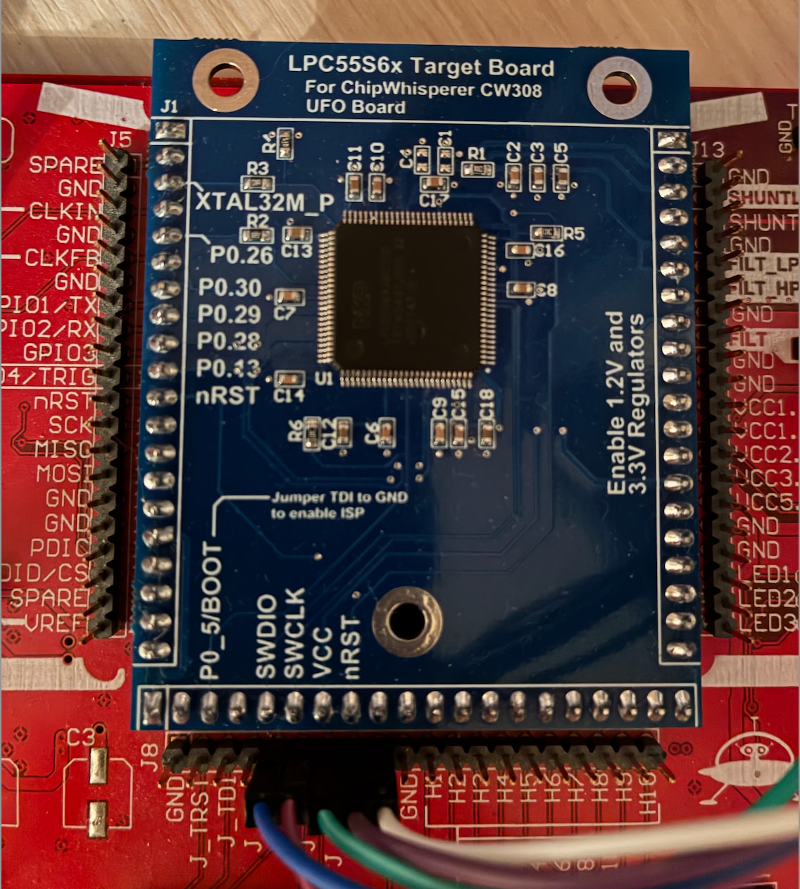
Another one thing I would like to highlight, all LPC55S69 in the marked are 1B version(where fixed a bunch of BootROM issues). So if one will decide to build the SW, it just won’t work due to many broken things (wrong clock configuration, wrong pin configuration). But it is pretty easy to fix. Also I increased the UART speed from 38400 to 115200.

As a result I was able to recover both AES-128 and AES-256 keys from the HW crypto.

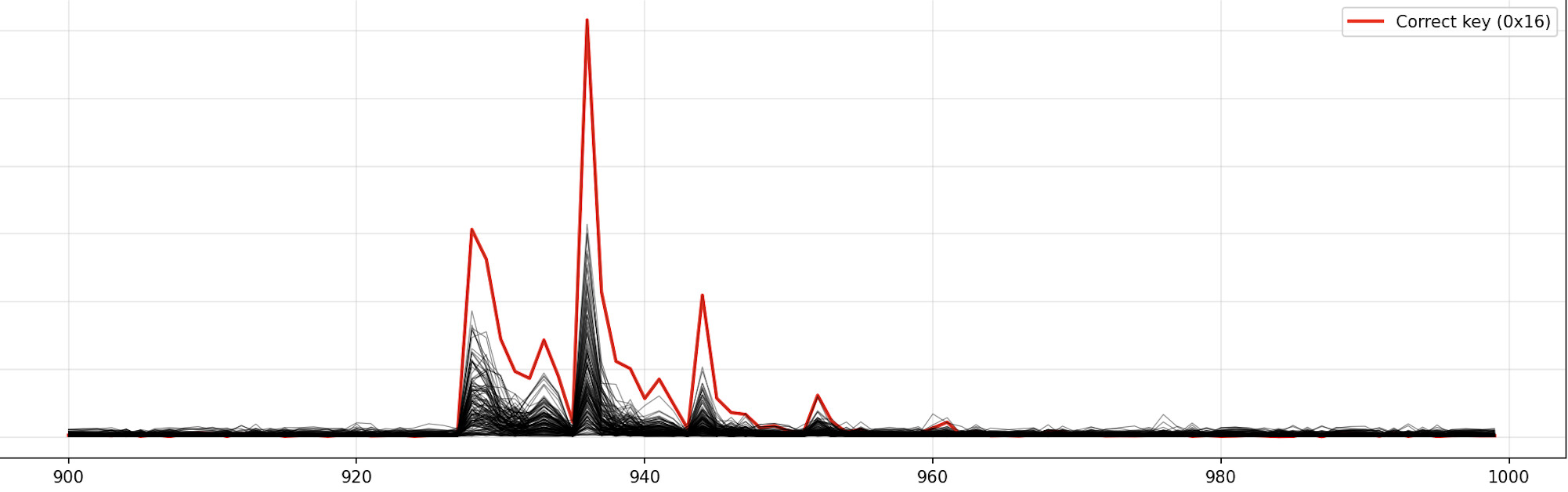
with 30000 power traces 14 bytes are clearly recovered. 8-th and 16-th key bytes are noisy. Increasing the power traces up to 100K makes possible to recover the whole key.

It worth to say, the Pearson correlation works bad here and I use my own approach.

The most interesting thing is masked AES. Surprisingly, the mask doesn’t affect key recovery at all. This is a question to NXP (what is the purpose of this mask if it doesn’t protect passing it explicitly via PUF_GetHwKey()).
So, I can say, it is definitely worth to try this target! You will learn a lot of things.

Actually, it’s currently in stock and available from Mouser:

https://www.mouser.ca/ProductDetail/NewAE/NAE-CW308T-LPC55S69?qs=PzGy0jfpSMt2GdLPAjxy4A%3D%3D

Sorry you encountered outdated gerbers, we will look into that.

Unfortunately, it is not available in the EU region. The status for this board is “Restricted availability“.

BTW, do you know what revision the SoC on these boards? 0A or 1B?

Unfortunately anything with hardware crypto can be subject to export controls, which complicates things. It’s not that we don’t want to make it available, we just haven’t gotten around to making that possible.

I’ve confirmed that we are using revision 1B.

I’ve updated the gerbers- thanks for noting that.

:+1:

…as I mentioned before the firmware should be fixed as well. There are several issues:

  1. As you confirmed the 1B revision is used now, the startup file and the linker script must be replaced (from new SDK) as the vector table layout was changed for 1B. Usage the existing startup file causes BootROM jump to the dead loop at 0x20006040 due to failed sanity checks.
  2. There should be added correct configuration for the P0.14 (trigger/GPIO4) and P0.28 (GPIO3) pins.
  3. There should be fixed clocking. I am not sure what clocking scheme was originally chosen but I guess ext clocking by 16Mhz using the bypass mode.
  4. I would recommend to increase the UART speed from 38400 to 115200 to increase trace collecting speed.

Hi @NewDwarf

Thanks for sharing your work on the LPC55S69. I’m investigating the encrypted firmware-update process on a device I own that uses an LPC5536JBD100, the non-S variant, not an LPC55S36 or LPC55S69. I would appreciate your thoughts on whether power side-channel analysis is worth exploring in my situation.

Here is what I have observed so far:

The update includes a valid P-256 point. Before the encrypted firmware payload is transferred, the update sends two 32-byte values, which I initially called A and B. Interpreted as big-endian X and Y coordinates, these form a valid point on NIST P-256 / secp256r1. The coordinate pairs from the firmware packages I examined satisfy the curve equation exactly, so this is more than a guess based on their size.

My working hypothesis is that this point is used in an ECDH-based key derivation process, and the resulting symmetric key is used to decrypt the firmware. I suspect AES-128, but I have not confirmed the AES key length, mode of operation, or key derivation function.

The A/B values differ between firmware packages. This makes me suspect that each firmware package has a different derived decryption key.

I expect the AES implementation to be software-based. My understanding from the LPC553x documentation is that this non-S part does not provide the hardware AES accelerator found on the secure variants. Therefore, assuming the payload is decrypted on the LPC5536 itself, I would expect software AES rather than the hardware AES implementation you examined. I have not verified the actual bootloader implementation.

The main constraint is the amount of data per update. The firmware payload corresponds to approximately 5000 16-byte blocks, so I would expect roughly that many AES block operations during one update, assuming the above interpretation is correct. To clarify, this is an estimate based on the payload size, not 5000 usable power traces that I have already captured.

I can repeat the same firmware update and collect additional measurements. However, that would mean measuring the same encrypted payload repeatedly, rather than obtaining additional distinct inputs. I’m not sure how useful those repeated measurements would be, particularly while key reuse between update sessions remains unconfirmed.

Does this interpretation of the update process sound reasonable, or am I overlooking an important alternative explanation? More specifically, would approximately 5,000 block operations per firmware image be a meaningful starting point for evaluating software-AES leakage, and would repeated measurements of the same update provide useful additional information?

Any insights or references to similar work on the non-S LPC553x parts would be greatly appreciated.

@jpthibault is there any instruction manual to program the device and collect traces?
I could not program the device with husky and cw313 board. the board is not getting detected. Need help here.

An external programmer is required, as we explain here: