Hi,
I have a question while I am modifying the CW308T_IMXRT1062 PCB.
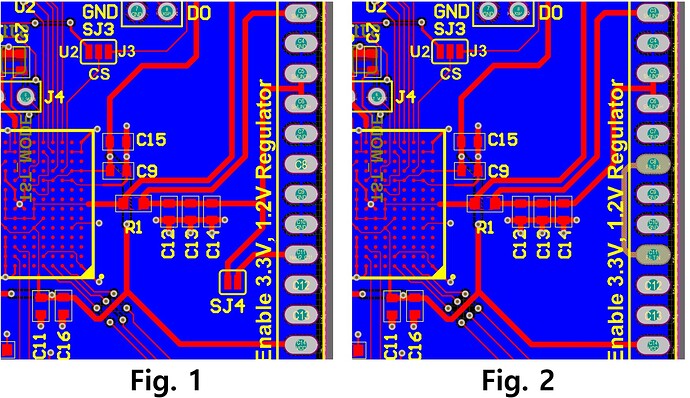
The following Fig. 1 is the existing PCB layout, and here, 1.2V is supplied directly to the core power VDD_SOC_IN through SJ4 instead of being connected to the filter input.
That is, the connection between the filter’s output (C5 and C6) and VDD_SOC_IN is meaningless.
Therefore, I connected it directly to the filter input (C8) removing SJ4 as shown in Fig. 2.
Would there be any problem with this modification?
Also, I am curious about the intention behind Fig. 1.
Thank you.
Yeah you’re likely right that changing to using the filtered input is fine. This is a WIP design from a few years ago, so I can’t really comment on why this was done, or whether or not the board works at all.
Alex
Thank you Alex,
I realized that the initial version of artwork created by @coflynn (marked as NOT TESTED) uses the filter, like Fig. 2.
Initial version: 62340e9 commit in here
But, in the next version, it was modified like Fig. 1 (which doesn’t indicate NOT TESTED here).
It seems that there may be problems with using a filter in CW308T_IMXRT1062.
Can you answer if the modified version (Fig. 1 above) has been tested @coflynn?
We never did a full release for that, so I admit we didn’t do extensive testing!
But normally that means the drop across the filter was too high & it was causing the device to brown-out or similar. The filter on the CW308 has a fairly high resistance, so if you try to draw too much current the drop across it can become a problem. It’s normally a bigger issue with 1.2V core targets like this, since e.g. they may be more sensitive to a 100 or 200mV drop than a 1.8 or 3.3V target will be.
Thank you for your answer Colin 
