I have a 256-BGA chip (NXP PowerPC) , which I’d like to glitch, however it’s stuck on a PCB now and it’s really hard tracing signals out. So I was thinking it may be a good thing to try to design a CW-UFO victim board. A few questions that popped up:
Do you have your Altium schematic library published? It will be a great help, as I don’t want to create a lot of footprints from scratch
Have you had any success with voltage glitching any PowerPC targets, such as SPC5748GSK1MMJ6? If so, is there a log of the procedure anywhere?
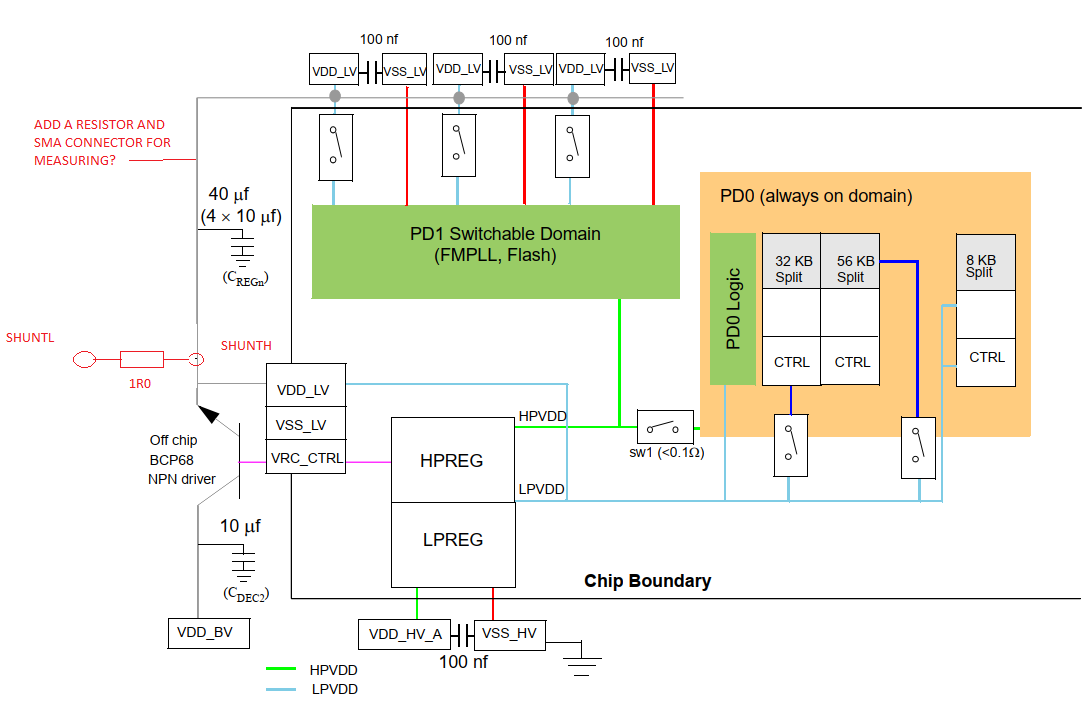
The chip I am targeting has a low-power domain which needs to be supplied by the internal chip regulator using an off-chip NPN driver. This is a requirement and supplying the chip with an external regulator is not allowed. This is not the case with SPC5748GSK1MMJ6, which is the target used in the CW board. I noticed that the glitch is inserted in pin K2 and any of the VDD_LV pins. For my application, I think I could glitch VRC_CTRL and any of the VDD_LV pins. Can you please comment on that?
I will also need to monitor the VDD_LV line with a scope (need to do power analysis as well), so I am thinking of adding a series resistor and an SMA connector to the line. That will need to be mounted on the target board itself
Could someone who’s familiar with the design of CW308T-MPC5748G comment?
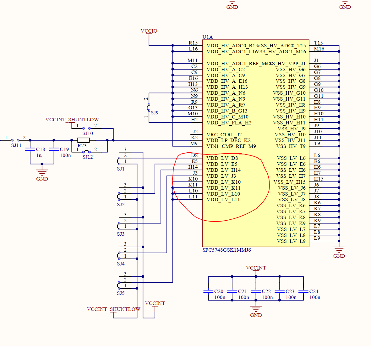
Some of the VDD_LV pins on the target are connected together, so they can only be glitched as a a single entity. The pins that are connected together are also physically close - was that the rationale behind the choice for connections to the glitch rail?
Also I’d like to know how to determine which VDD_LV pin supplies the CPU, which supplies the Flash and so on - is that possible at all?
Finally, I’d really appreciate if someone shares their experience with glitching either the BAM/BAF or JTAG access.
As a quick note - you can often supply external power no matter what they claim. In your schematic just sending a voltage into VDD_LV should work I think? I think the MPC5748G has the same design (if not the 5777C/5676R does, one of them does).
You sometimes need to trick the system into thinking it’s supplying external power. If they have a separate feedback pin (I don’t think this does?) that is great as you can drive just the feedback pin with a higher voltage and it effectively shuts off the internal regulator.
Yes it was for routing purposes that I connected the four together. I’m not sure how they all route - sometimes the datasheet will mention if there is separate pins as well - to be honest I don’t 100% recall if I found that documentation, looking at the ball map I think I just took all the balls that were “way out there” and made it possible to attack that pin separately. I didn’t verify if that actually matters or not though.
You can try checking resistance on the device too - if the pins are connected on the BGA carrier PCB, it may show as very low resistance, compared to if it’s on the die itself. Depending on the device package you may even be able to see traces on the BGA carrier PCB (but may require decapsulation).
I don’t really have logs of this - I’ve only done some experiments with ‘standard glitch examples’, but it didn’t work super-well even then. I had much better success with EMFI, but I haven’t spent a lot of time on this device. I’ve seen others who have had success, but I’m not sure if it was published. Thus I know it’s possible for voltage-FI to succeed!
All the automotive stuff seems to get weird as there is a lot of demand for ECU tuning that makes people want to keep it secret for commercial reasons. Partially I haven’t pushed as hard in this area as I get a lot of annoying emails about people wanting to do ECU tuning too that I ignore… and thats without publishing very much.
Hi @coflynn , thank you for the comprehensive response.
I’ve included a set of terminals for feeding external voltage to the VDD_LV domain of the MCU with the intent to vary it out of specs, hopefully that will aid the glitching in a way. The controller does not have a feedback pin, but I appreciate your note on disabling the internal VREG - that will certainly come in handy with other targets.
The MPC5xxx appears to be a hard nut to crack so far.
That can be helpful! Sometimes running it just at the edge of stability is a good starting point, with this one again I didn’t play too much in that area. Good luck!
The adapter boards have finally arrived and I’ve populated one of them with a brand new MCU, and set the JTAG password protection. Now it’s go time.
I tried to perform a basic power analysis on the supposed password checking procedure after sending the JTAG password - no success, but I haven’t spent a lot of time on that.
The BAM is not an option as that particular MCU performs the password check when the RAM loader has been downloaded, so at least at first glance it appears that the JTAG password checking is the only field that may yield results. Unfortunately the maximum number of JTAG unlock attempts is limited to 4 per second, as the device needs reset if you shift a wrong password, and the reset takes approx. 250 ms.
Any thoughts/ideas on how to proceed would be great.
From what I’ve seen most work has looked at F-I on the password comparison results. What I would concentrate on is how the power trace looks after sending a correct vs. incorrect password (you might need custom triggering here).
I’ve collected a large array of traces while the processor is supposedly processing the JTAG password. There’s no observable difference with the traces of the wrong password; moreover, traces seem random. I do use triggering on JTAG clock line (with the help of a JK flip-flop and RPi Pico), and also scope the power line to ensure I am not capturing garbage.
Is it possible that the JTAG state machine is implemented as a separate logic block, and does not make use of the CPU? That would explain why JTAG activity does not appear in the processor power trace, and works well with external clock.
That being said, there are more things to try:
If the JTAG interface is a separate logic block, it would still need to read the password from the shadow flash at some point; maybe the memory read operation uses more power than the usual CPU activities
The processor probably reads the state of the JTAG interface after boot and that may be a good point to glitch
Edit: There’s at least one more strategy:
Try to glitch the BAM, as described by Colin in BAM BAM What’s making this a non-preferred approach is that the MCU actually does the password comparison after the RAM loader has been downloaded (it’s from the SPC variety). The download itself takes quite some time over UART. I’d need to write a minimal RAM loader image, which reads the shadow flash password only. If someone has experience with that, please share your thoughts.
 What’s making this a non-preferred approach is that the MCU actually does the password comparison after the RAM loader has been downloaded (it’s from the SPC variety). The download itself takes quite some time over UART. I’d need to write a minimal RAM loader image, which reads the shadow flash password only. If someone has experience with that, please share your thoughts.