I am working with the ChipShouter and the Ballistic gel board on a research project at University Laval.
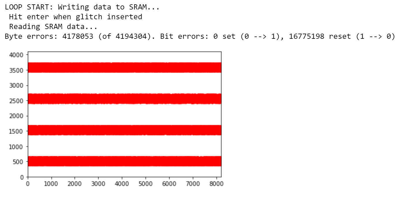
We have been playing around with the Ballistic Gel target with the Python program available on GitHub. I have enable the option “doplot = True”. And what I get is a physical mapping of the SRAM chip with the location of the injected faults in red. Am I correct?
The thing that has been puzzling me is that when I inject a fault in the center of the chip with the ChipShouter at a high voltage, almost every bytes of the memory are corrupted. However, it displays a red and white stripping pattern on the plot. In other words, the faults are concentrated on stripes rather than being spread across the whole surface of the SRAM as shown in the attached image
From what I remember, we could never quite figure out how the SRAM addresses mapped to actual areas on the chips. I tried a bunch of mappings, and got stuff that looked promising, but never really came together.
Yeah the plotting is a a little odd - so the mapping comes from Alliance themselves, and they claim it’s fully accurate. However at some point I stopped getting good info - the mapping isn’t something they would normally share, and I wasn’t going to be a #1 customer for them they figured out eventually…
If you crank the power up it becomes almost totally meaningless we found - I suspect you’re seeing stuff like errors propagating across entire word lines & power rails.
There was an unknown about the mapping of the AS6C3216 vs AS6C3216A, as the documentation I had was unclear (was told it’s for AS6C3216A but marked as AS6C3216). Ultimately the XY mapping is left a little open - I had someone physically imaging the chip for me to try and work this out, but it was still non-trivial to reverse engineer the actual addressing & world-line blocks from there.