I got done setting up my Chipwhisperer-Lite, and got it updated. Now I’m going through the courses. I noticed in Courses, Fault101, Fault 1_1 - Introduction to Clock Glitching, on the 4th figure, the circuit doesn’t match the timing diagram. I added it below.
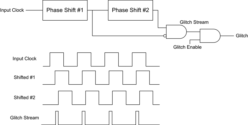
Since the phase shift clock #1 gets inverted before the AND gate, the ‘Glitch Stream’ should be high, when phase shift clock #1 is low and phase shift clock #2 is high. However, ‘Glitch Stream’ is high, when phase shift clock #1 is high and phase shift clock #2 is low. Making the circuit not match the timing diagram.
I’m an electrical engineer, and I have wrote thousands of pages of A-specs, D-specs, and C-specs. I have made tons of errors myself. I noticed this and wanted to make NewAE aware of the error.
Also the numbering of the phase shift clocks are wrong. Should be 0 & 1, instead of 1 & 2 (I’m joking about this, as it is EE humor).
A quick suggestion on an improvement to the clock glitching circuit above. It might be useful to invert the 2 phase shifted clocks independently. Two new registers would be needed, and then use something like scope.glitch.ph_clk[1:2]_inv = False(default)\True. Then the regs could drive the select pins of 2 muxes, that selects the clocks, or inverse of the clocks. Or a better solution might be 2 XOR gates, instead of 2 muxes and 2 inverters. The clock connects to the first input of the XOR gate, and the reg connects to the second input. When the reg is 0, the output is the clock. When the reg is 1, the output is the clock inverted. I don’t know which is easier or harder to implement in a FPGA. I guess it depends on what logic is closer, and how it affects the timing, if there is space and gates available. Never done FPGA stuff, so I don’t know, or even if it can be added with changes to the VHDL/Verilog code.
Darren