Hello everybody,
I have some free time again, so I’m getting back to glitching. In the past I worked on CWLite, now I have moved on to Husky. I am currently trying to work on a real target, the NXP 5169 (https://www.nxp.com/docs/en/data-sheet/JN5169.pdf). I am trying to do some voltage glitching but without success.
The initial scheme is similar to the following.
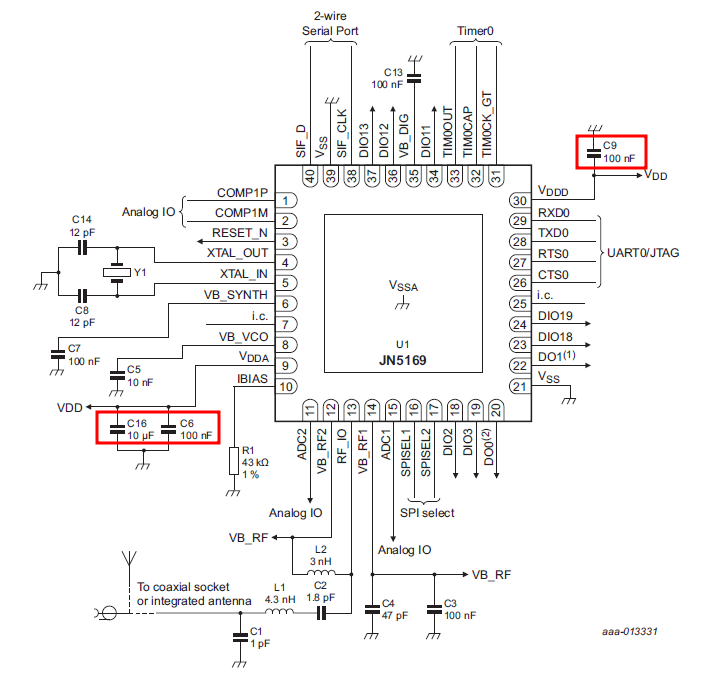
In red I have already highlighted the capacitors, what is not clear to me is if I have to remove them all or only the C9? VDDD is the digital circuit voltage supply, VDDA is for the analog part.
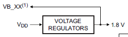
On the datasheet I saw also that there is a voltage regulator.
The device is powered from the VDDA and VDDD pins, each being decoupled with a 100 nF
ceramic capacitor. VDDA is the power supply to the analog circuitry; it should be decoupled
to ground. VDDD is the power supply for the digital circuitry; it should also be decoupled to
ground. In addition, a common 10 F tantalum capacitor is required for low frequencies.
Decoupling pins for the internal 1.8 V regulators are provided with each pin requiring a
100 nF capacitor located as close to the device as practical. VB_SYNTH and VB_DIG
require only a 100 nF capacitor. VB_RF1 and VB_RF2 should be connected together as
close to the device as practical, and require one 100 nF capacitor and one 47 pF
capacitor. The pin VB_VCO requires a 10 nF capacitor. See Figure 48 for a schematic
diagram.
In this case, the capacitors positioned after the voltage regulator (substantially on the VB_XX lines, C2, C1, C4, C3, C7, C13) could affect the ability to perform glitching?
Furthermore, since I have the VB_XX pins available, does it make sense to glitch on the VDDD or does it make more sense to go and do it on the VB_XX after the voltage regulator?
Thank you in advance