When voltage glitching, i know its possible to crank up the clkgen_freq so that you can potentially glitch beginning anywhere within a lower speed clock. I also know that when clock glitching, you can use offsets and widths to move to various points in a clock cycle. What I’d like to know is if there is some way to increase the clkgen_freq when you are providing the clock on HS2, but not alter the target frequency. So, for example, if the target was 8Mhz, and you wanted to put multiple glitches, say 2, into one cycle, while CLOCK glitching, is there a way to crank up the glitch clock to 16MHz, but keep the target clock at 8MHz. I can’t seem to figure out a good way to achieve this, other than to come up with some additional clock circuit that the target and the cwpro 1200 can sync from.
Sort of, but not in an ideal way – if the target is sourcing the sampling clock from HS1 (I originally wrote HS2 – sorry for the confusion!), then you can set the glitch module’s clock source to clkgen and have that be some multiple of the HS1 clock, however these two clocks won’t be locked and can drift apart. BTW you can do this whether you’re doing voltage or clock glitching; the glitch generation logic is exactly the same for both cases.
Out of curiosity, is there any literature on the efficacy of these types of glitches? If it’s something that’s shown to be effective, we could consider updates to the FPGA Verilog code to make this possible. In theory this should be easy to do, but in practice it can be tricky with all the different clock domains and the fact that glitch generation uses clocks in a very unusual way.
Jean-Pierre
I wish there were MORE literature or at least examples of glitching in general. I’ve combed the web and your site for different setups. And while all seem to show a lot of promise, trying to duplicate another person’s results has been difficult. Before the CW1200 even arrived, I attempted to make my own “crowbar glitcher” with success in creating something that could work, but I didn’t have anything to synchronize it well enough to hit anything I was trying to target. I’ve been working with the CW1200 for a bit now and my first goal is to try and make a glitch I generate as reliable as I can make it. So I’m currently going through the examples that you have. As I was reading through the information on voltage glitching, it occurred to me that if I could up the clock, by 2 or by 4 times that of my target, it might be more accurate as far as targeting a glitch in a known clock cycle, possibly making something easier to reproduce. But I have no solid way to test that or prove it one way or another. Ultimately, it may be no more effective that increasing or decreasing the width and moving the offset. If in fact, as you say, the two clocks will drift appart quickly, then this might be far less effective. i was hoping the two could be more closely synchronized, but this isn’t always easy. My other thought though was that it might be easier to glitch a target if you could get it to think of one clock cycle as 3 or 5 clocks instead (two glitches in one clock generating 3 “clocks” and 4 glitches generating 5 “clocks”), especially if you need to skip a multi-cycle instruction before some other piece of external hardware does something. But, as it is pointed out somewhere in your documentation, this isn’t an exact science, so it is possible that this wouldn’t work well at all and being able to generate a larger swath of glitches produces more reliable glitches, if not always desirable results.
Anyway, if I understand everything correctly then, the HS2 output clock can be generated from, say, the HS1 input (i.e. the target) and I can then clock_xor in the glitch and run the glitch from a 2xTarget by providing say 2x the frequency into clkgen_freq? So if I understand this, the glitches may drift around in a clock cycle (as the clkgen clock drifts away from the target)… Or can I attempt to lock the clkgen_freq to the target by sourcing clkgen from the target AND sourcing HS2 from the target, but increasing clkgen_freq to say 2x or 4x the target clock. Which I assume will still drift as the PLL drifts (I don’t know what the drift rate on these PLLs are)
First, I edited my post above because I wrote HS2 when I should have written HS1 – sorry for the confusion.
Glitching is definitely part art and part science!
If ChipWhisperer is locked to the target clock, then using a multiplied clock shouldn’t have any effect on the glitch timing accuracy. It’s not going to be always exactly the same; this will depend on the jitter present on the target clock, and the degree to which the Xilinx DCM blocks used to generate the glitches filters that jitter, so no easy answer there. Using a multiple of the clock won’t change that. One way to deal with that is to repeat the same glitch parameters multiple times.
On the other hand, introducing an independent clock which isn’t locked to the target clock can make reproducibility much more challenging: in addition to jitter there is now clock drift, and the fact that the two clocks may not even have the exact same frequency. I would avoid that if at all possible.
Now I had forgotten that there is one thing you can do in the case of a target-sourced clock. This only works if the target is generating its own clock (e.g. it is not sourced from ChipWhisperer). You would set
scope.clock.clkgen_src = 'extclk'
scope.clock.adc_src = 'extclk_x1' #(or extclk_x4)
scope.glitch.clk_src = 'clkgen'
Then, set scope.clock.clkgen_freq to a multiple of your target’s clock. The glitch module clock will then be phase-locked to the target clock.
Finally, I think you know this but do keep in mind that with the clock_or and clock_xor modes, it is possible to get two glitches in one clock cycle when glitch clock == target clock.
I realize there are so many options around clocking and glitching and it’s easy to get confused (myself included!). I’m going to try put together a demo notebook which allows the glitch output to be visualized. I’ll update here when that’s ready.
Actually, what would be really helpful, although I know difficult to reproduce with little person-power would be something where the setup parameters are read and a simple visual diagram of what you are actually doing would help immensely. Basically, something that shows the clock path to all the different areas and indicates something like “x2” or “x4” where appropriate.
What you describe here is essentially what I was trying to do, but it wasn’t clear that the output “HS2” could ultimately be “independent” of the target clock speed just by setting the frequency. I looked at the diagram over and over and for some stupid reason it just didn’t dawn on me, until I read another post somewhere here, that the frequency of the glitch can really be higher than the target… So, is HS2 dependent on the ADC pll and the glitch clock dependent on the CLKGEN pll? That’s how I. am understanding that now. I know I’ve looked at the clock generation diagram several times, but I just overlooked which PLL ultimately drives what, and that seems to be the most important.
My ultimate target has an internal clock, so I’m kind of “screwed” as far as getting anything “clock accurate”… but its possible that the internal clock is ignored when driven from outside (according to the datasheet). So I might be able to depend on the external crystal. My ultimate target is an STM32F205… This will be the first real “hard target” I’ve tried to glitch. I have a soft example (i.e. no protection), but there are a lot of issues. I’m trying to remove as many as I can because I’ve been able to dump the bootloader of the soft target and it appears that if I wish to dump any real data, I’ll have to be able to perform multiple glitches accurately (which may just not be doable… I don’t know).
I’ve been able to glitch the examples from the chipwhisperer as well as some others, but ACCURATELY enough to build anything around it has me stymied for now. Because of this, I’ve gone back to the examples, to try to work through them again to see what and where I’m missing things. You’ve actually been a big help because I’ve been able to work out a few details in my own head that were lacking.
Have you seen these diagrams from our readthedocs site?
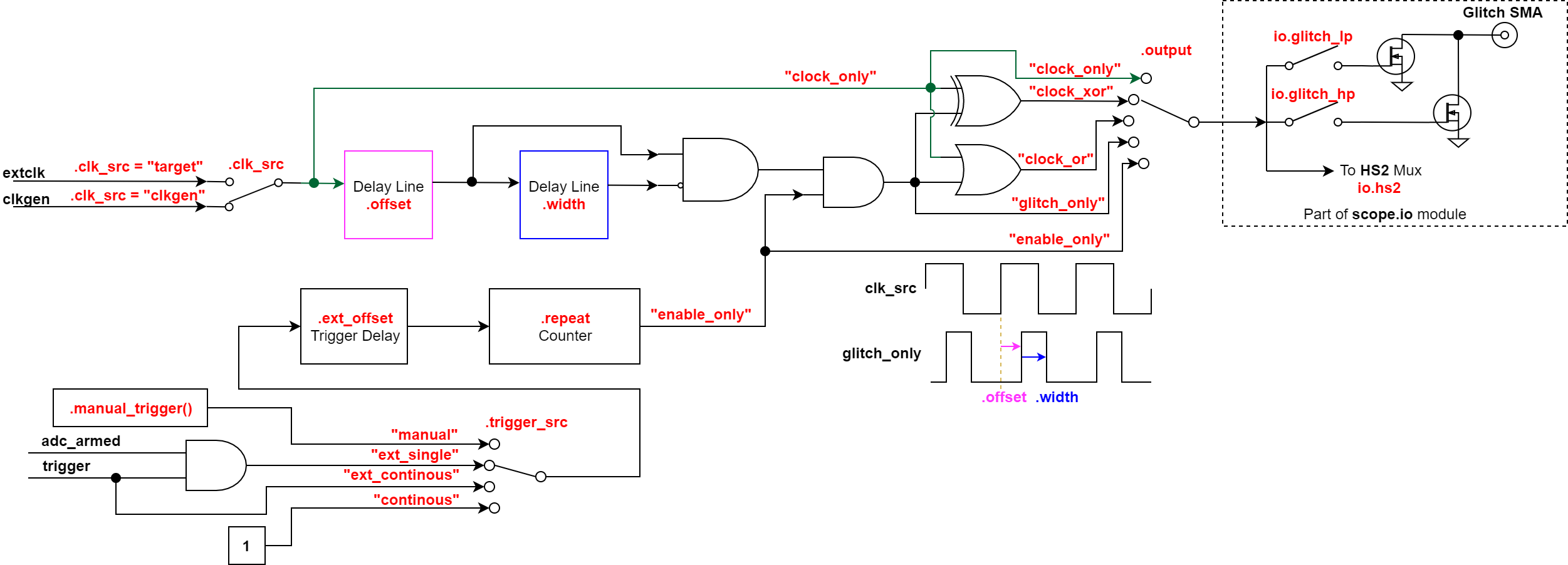
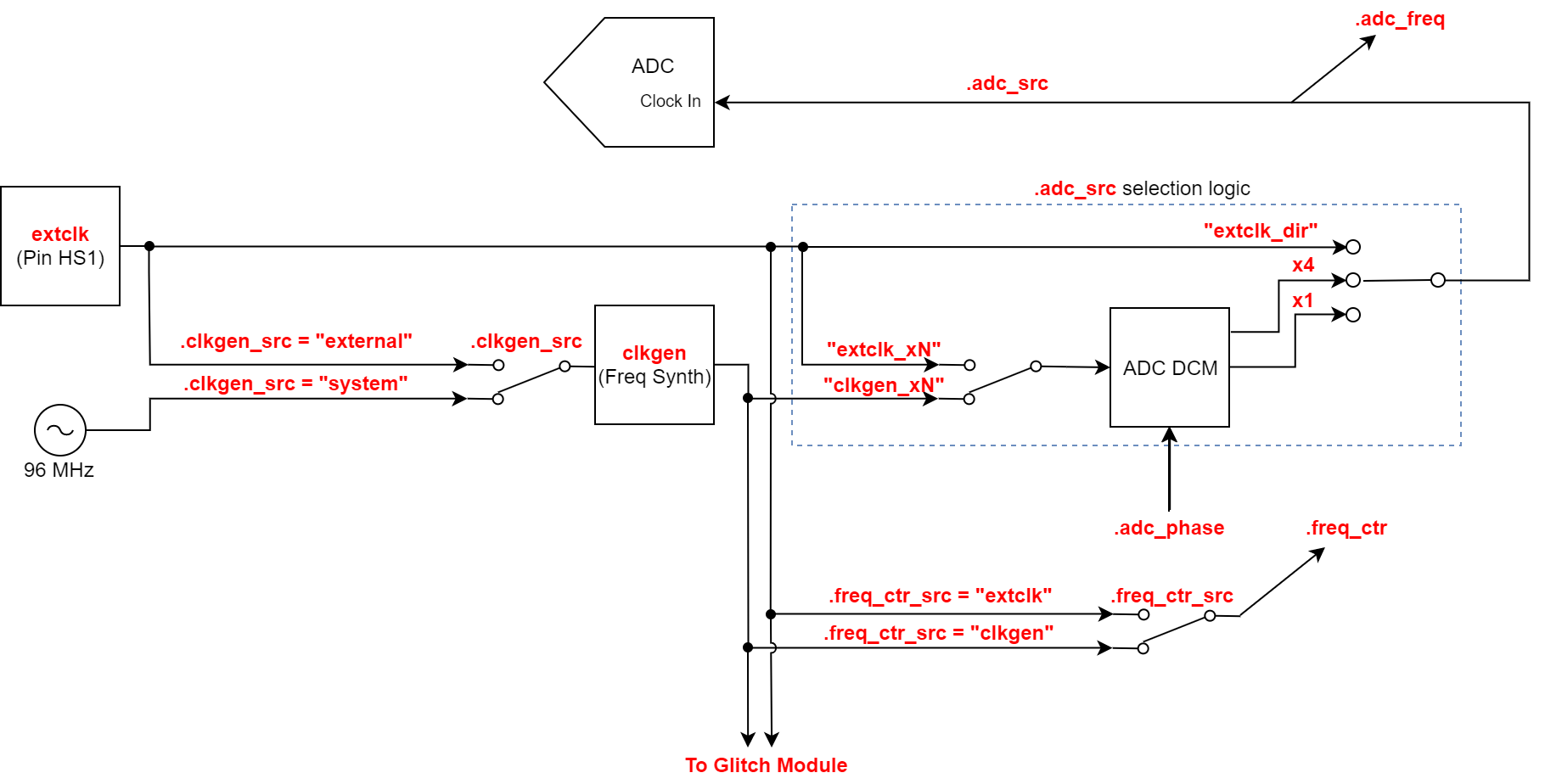
I think these cover everything, but let me know if not – sometimes things that are obvious to us are not so clear to others.
Jean-Pierre
Yeah, those are the diagrams I was referring to above. I see the HS2 essentially being driven by HS1… And the external and clkgen both head to “glitch” for “xor” presumably. So that is pretty much doing what I wanted to do (if you double the clkgen it generates two glitches per cycle)… and its “locked”. I think that is what I set up (at least from what I’ve done so far), but the issue I then have is that the ACM0 frequency is now changed… I tried to fix THAT based on another example I was looking at, but I always get garbled output (the code that I had looked at had shown someone basically taking the 7.3MHz crystal and dividing that into 24 and multiplying by the baud rate to get the new baud rate). So it was something like this:
baudrate = 38400 * 24 / 7.37
I tried that example, and it worked (they were generating a clock into the system that was 24MHz, so hs2 was 24MHz out)… No issues with the baud rate. But when I tried to adjust the baud rate based on my frequency (say 7.37*2)… it generates 768xx.xxxxx for the baud rate, which appears correct, but when I check it in the terminal, its always off. Currently I’m trying to run some tests with the STM32F303 and the basic code from Chipwhisperer, but I can’t trigger on DECODE_IO if I’m getting junk from the serial port. But it appears I may have the clkgen and ADC plls backwards as I set things up a little differently and the baudrate has pretty much cleared up. I see now that if I set the ADC to extclk_4 and let the clkgen frequency remain whatever comes in, then I essentially get what I was looking for. If I leave it at x1, then I get 1 glitch. Otherwise I get 4 glitches. I guess I don’t have an x2 or x8 clock, but that’s ok.
I’m currently at the stage where I’m trying to delve into the chipwhisperer examples, (especially the first clock glitching example, to make sure I understand all the details. The notebooks worked somewhat. But I know that in the future I’m going to have to work out other issues and I’d rather do that in an environment I can control.
I might have misunderstood something… what is your target clock now?
What exactly do you mean when you say that the baud rate is “off” in the terminal; what are you observing? (ideally can you check it with an external logic analyzer?)
You’re right that if you change the target clock from its default 7.37MHz, you’ll need to adjust target.baud accordingly. But you’ll also have to adjust scope.decode_IO.rx_baud.
Jean-Pierre
I fixed the issue. Since I ultimately had the two clocks switched in my head, I was trying to adjust the clkgen freq… this just garbled the serial io, no matter what I did. As soon as I switched the clocks and increased the ADC clock (with ‘extclk_x4’) and left the clkgen clock frequency alone, the serial port was fine. I believe I’m ultimately getting what I was wondering about at first (4 glitches per clock), but NOW I don’t have any baud rate issues.
Actually, I’m getting good, repeatable results from the first setup. It seems that turning off all of the extraneous power sources (1.2, 1.8, 2.5, and 5.0) really seems to help for the STM32F303 target (even if you aren’t using the variable power)…