Improving SNR and Mitigating Ground Bounce during CPA on I2C Devices (CW313 + Husky)

Hello everyone,

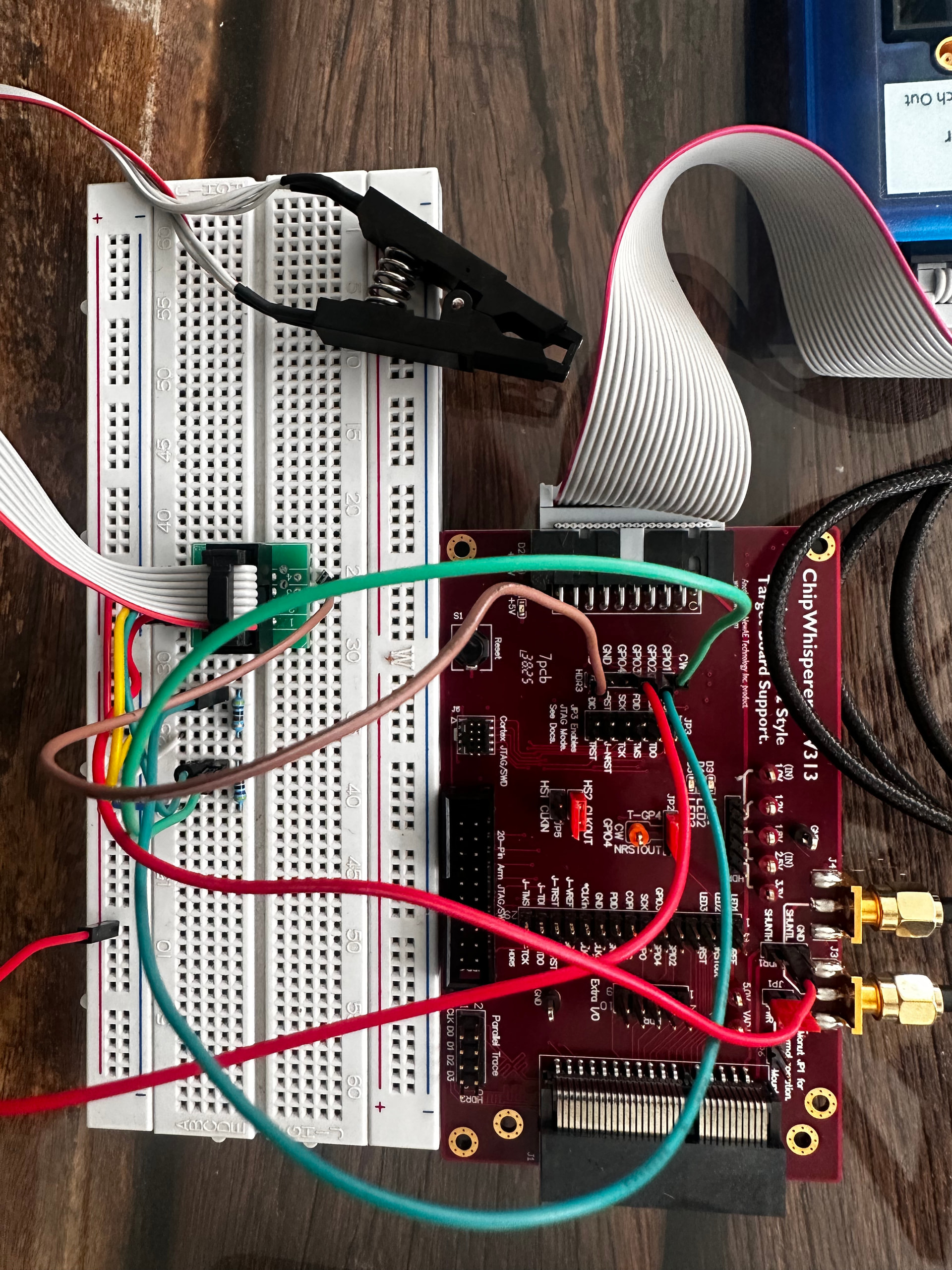
I am a beginner in the SCA field, currently conducting academic research on I2C state-machine behavior using the ChipWhisperer-Husky Starter Kit. I am working with a custom breadboard setup alongside the CW313 Interposer Board.

My research involves analyzing the power consumption of an EEPROM (AT88SC family) during specific I2C transactions. To study the reset state of the chip’s internal logic, my experiment requires power-cycling the target device abruptly before an I2C STOP condition is generated.

While the logic side of my Python script works, I am facing severe analog and synchronization issues (poor SNR and ghost peaks) and would appreciate some guidance from the community on how to improve my hardware setup.

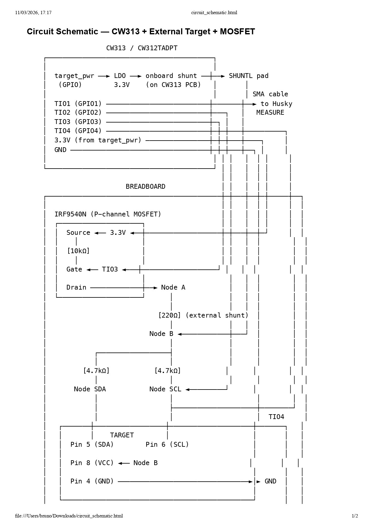
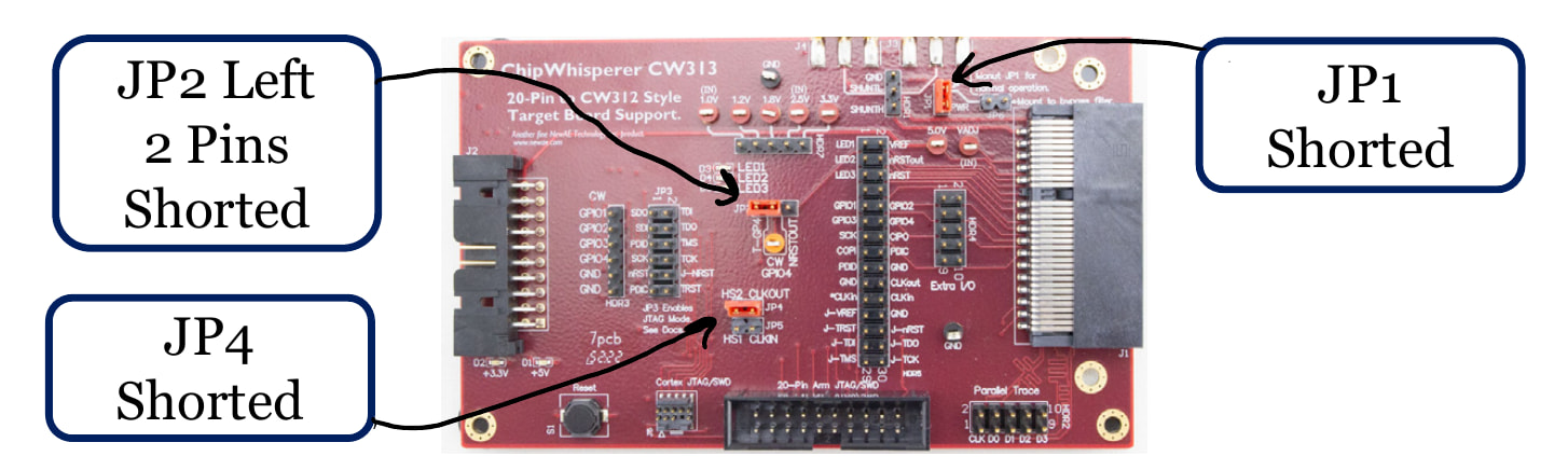
1. Hardware Setup (CW313 ↔ Breadboard)

Since I am bit-banging the I2C protocol, I am using the CW313 to bridge the Husky and my breadboard:

  • Target: 8-lead SOIC connected via micro test clips to a breadboard.

  • I2C Comm: CW313 GPIO01 (Husky TIO1) → SDA | CW313 GPIO02 (Husky TIO2) → SCL.

  • Pull-up Resistors: Two 4.7kΩ pull-up resistors on SDA and SCL. I am using CW313 GPIO03 (driven HIGH via Husky TIO3) to feed the 3.3V rail powering these pull-ups.

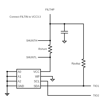
  • Power Measurement: I am using the CW313’s onboard shunt. The SHUNTL pin goes directly to the target’s VCC. I am using Husky’s 3.3V Target Power (scope.io.target_pwr) to power the board. Toggling this pin allows me to power-cycle the target.

2. The Analog Problem

Because I am abruptly power-cycling the target during the experiment:

  1. Ground Bounce / PLL Issues: When target_pwr is set to False, the resulting ground bounce causes the Husky’s ADC/Glitch LEDs to blink. The FPGA reports target clock issues (even though clkgen_src = 'system').

  2. Correlation Issues: I am applying FFT alignment on the traces. However, the CPA (Pearson Correlation with Hamming Weight) models are returning erratic peaks (e.g., 0x12, 0x7A). I suspect the power cut transient is completely destroying my SNR, or the bit-banged I2C clock pauses are misaligning the capture window.

3. The Implementation

Here is the core logic I am using. I am arming the scope at the 8th bit of the payload, right before the ACK cycle.

import chipwhisperer as cw
import time
import numpy as np
import scipy.signal

1. SETUP

scope = cw.scope()
scope.default_setup()
time.sleep(0.5)

Shielding the Husky clock for I2C Bit-Banging

scope.clock.clkgen_src = ‘system’
scope.clock.clkgen_freq = 7372800
scope.clock.adc_mul = 4
scope.glitch.enabled = False
scope.clock.reset_adc()
time.sleep(0.5)
scope.errors.clear()

scope.trigger.triggers = “tio4”
scope.trigger.module = “basic”
scope.gain.db = 25
scope.adc.samples = 15000
scope.adc.offset = 0

Power the pull-ups via CW313 GPIO03

scope.io.tio3 = “gpio_high”

def sda(bit): scope.io.tio1 = “high_z” if bit else “gpio_low”
def scl(bit): scope.io.tio2 = “high_z” if bit else “gpio_low”

def i2c_experiment_capture(data_byte):
for i in range(7):
sda((data_byte >> (7 - i)) & 1)
scl(1); scl(0)

sda(data_byte & 1)
scl(0) 

# Arm the scope right before the operation
scope.arm()      
scope.io.tio4 = "gpio_high"
scope.io.tio4 = "gpio_low"

scl(1)
scl(0) 
time.sleep(0.002) # Wait for recording to finish

sda(1); scl(1)
ack = scope.io.tio_states[0]

# Hold SCL low to prevent I2C STOP condition before power cycle
scl(0) 
return ack

2. CAPTURE LOOP

num_iterations = 256
traces = np.zeros((num_iterations, scope.adc.samples))

for iteration in range(num_iterations):
temp_traces = 


for _ in range(10): # Captures per iteration
    scope.io.target_pwr = True
    time.sleep(0.05) 
    sda(1); scl(1)
    time.sleep(0.01)

    # Standard I2C Start and setup bytes
    sda(0); scl(0)             
    # ... (sending setup bytes) ...
    
    i2c_experiment_capture(iteration)
    
    ret = scope.capture()
    if not ret:
        trace = scope.get_last_trace()
        if trace is not None and (np.max(trace) - np.min(trace)) > 0.01:
            temp_traces.append(trace)
    
    scope.errors.clear() 
    
    # Power cycle target to study state machine reset
    scope.io.target_pwr = False     
    time.sleep(0.05) 
        
if len(temp_traces) > 0:
    traces[iteration] = np.mean(temp_traces, axis=0)

(Standard FFT alignment and CPA math follows…)


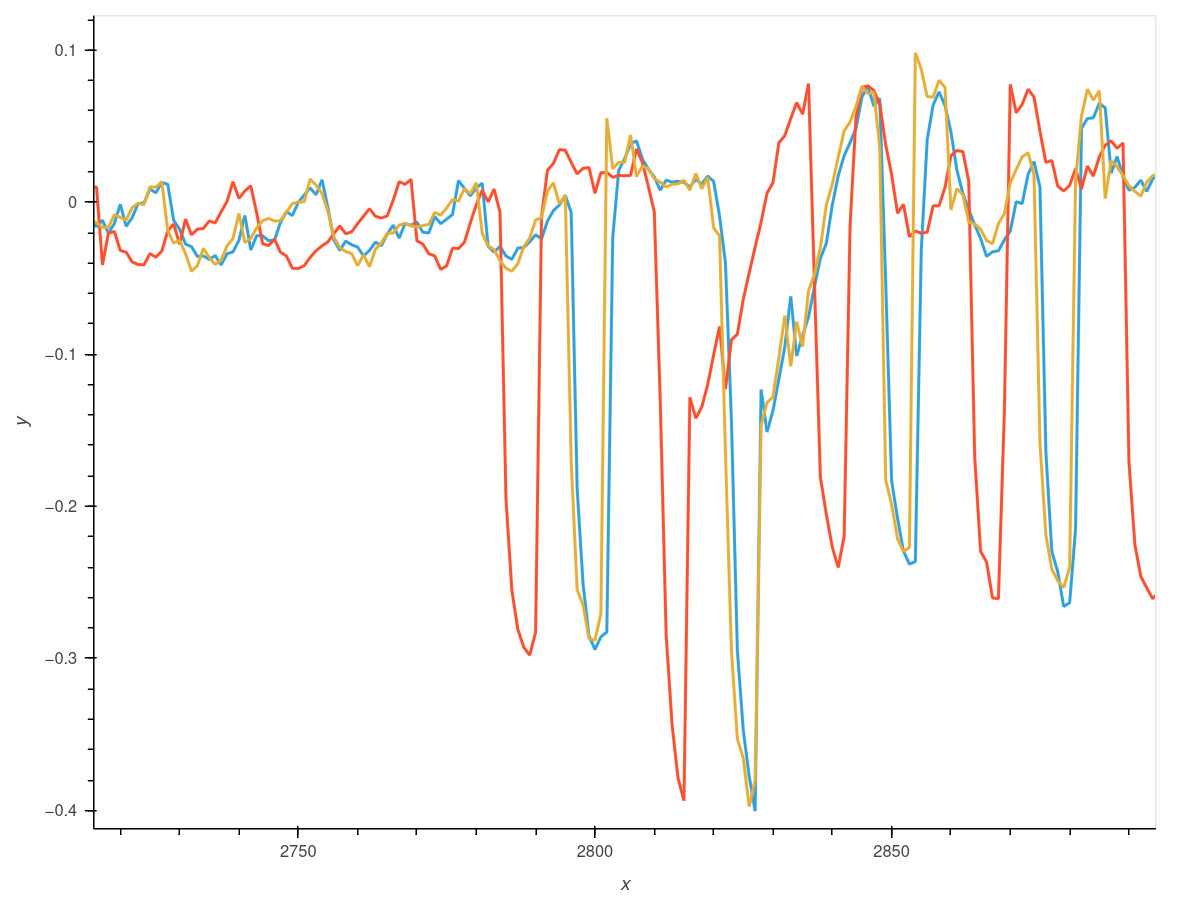
My Question: Is this reasoning appropriate for measuring analog data during state-machine interruptions? I would greatly appreciate suggestions from experienced members on how to adjust the Husky ADC settings or improve the hardware measurement to prevent the ground bounce from corrupting the SNR.

Thanks in advance!

Hello and welcome.

This doesn’t give me a full picture of your setup; a schematic would be useful.

What exactly is the error? Run print(scope.errors) to find out.

What exactly are the “target clock issues”?

Hello, and thank you for taking the time to reply!

To give you a better picture, my target is an Atmel AT88SC25616C (CryptoMemory). My goal is to extract a 24-bit password by exploiting a timing/power leakage in the EEPROM’s charge pump activation, combined with a “Tear-Off” attack to prevent the internal security counter (PAC) from decrementing.

Here is the breakdown of the setup, the errors, the progress I’ve made, and the analog wall I’ve hit.

1. The Setup & “Schematic”

I am using a custom breadboard connected to the CW313 Interposer.

  • Target: AT88SC25616C (8-lead SOIC).

  • VCC: Routed directly through the CW313 SHUNTL for power analysis. The power is supplied by Husky’s target_pwr.

  • I2C Bus: Bit-banged. TIO1 → SDA, TIO2 → SCL.

  • Pull-ups: Two 4.7kΩ resistors, powered by TIO3 (driven HIGH).

  • Trigger: TIO4 is pulsed HIGH->LOW right before I send the I2C STOP condition.

  • The Tear-Off: Exactly 3.5ms after the STOP condition, I hard-cut the power (scope.io.target_pwr = False) to prevent the EEPROM from finalizing the PAC decrement write cycle.

2. The Errors & Target Clock Issues

When I run print(scope.errors) right after the power cut, I typically get an ADC Error (specifically, ADC clipping or phase errors) and sometimes ExtClk Error.

Because I am abruptly dropping target_pwr while the pull-ups and logic lines are still active, it creates a massive ground bounce/transient. Even though I am using scope.clock.clkgen_src = 'system' (the Husky is generating its own clock, not relying on the target), the electrical shock on the CW313 seems to destabilize the Husky’s ADC PLL or trigger logic momentarily, causing the LEDs to flash red.

3. The Attack Progression & The Core Problem

Despite the transient, I managed to capture clean enough traces before the power cut to successfully extract the 1st byte of the password, but the 2nd and 3rd bytes completely broke my mathematical models.

The State-Machine Leakage: When the chip verifies the 3-byte password, it evaluates them sequentially.

  • If Byte 1 is wrong, it immediately fires up the high-voltage charge pump to write to the EEPROM (decreasing the PAC).

  • If Byte 1 is correct, it delays the charge pump ignition to check Byte 2. This creates a beautiful, measurable delay in the power trace (Timing Leakage).

The Success (Byte 1): Using a simple TVLA and a Single-Point DPA (or SAD), I successfully isolated Byte 1 (0x18). The charge pump ignition happens early enough (around sample 30,000 at 29.5 MS/s) that the traces align well.

The Analog Wall (Bytes 2 & 3): The AT88SC relies on an internal, asynchronous RC oscillator running at ~36 kHz. By the time the execution reaches the Byte 2 decision (around sample 50,000+) and Byte 3 (sample 60,000+), the thermal and voltage variations cause massive Cumulative Phase Drift.

When I visually inspect the traces, I can clearly see that the correct Byte 2 (0xC4) holds the baseline voltage steady while all other 255 incorrect guesses suffer a voltage sag (charge pump activating). However, because of the severe jitter and DC offset between captures, standard Time-Domain Analysis (SAD, Variance, CPA, or Threshold Crossing) completely fails. The mathematical models end up latching onto noise spikes or baseline drifts rather than the actual charge pump delay.

4. What I Need Help With

To make this project successful and reliable, I need guidance on two fronts:

  1. Hardware / Measurement: How can I cleanly cut power to the target (Tear-Off) without causing a transient that crashes the Husky’s ADC? Should I use an external MOSFET circuit triggered by a GPIO instead of dropping scope.io.target_pwr directly?

  2. Software / Signal Processing: Standard FFT alignment on the start of the trace doesn’t fix the asynchronous RC drift 60,000 samples later. What are the best practices within the ChipWhisperer ecosystem for aligning traces with severe internal clock jitter? Is implementing Dynamic Time Warping (DTW) or Elastic Alignment the only way out, or is there a better feature-extraction technique for this kind of asynchronous delay?

Thank you again for the support!

Let me first set expectations: we cannot answer all your questions, particularly on the signal processing side. We answer all questions directly related to using our products. We’re happy to help with questions that fall outside of that, so asking such questions is not a problem, but understand that we may not be able to help you with e.g. aligning your traces. Doing this well can require pretty deep knowledge about your setup, your target, and your goals, and that’s well outside the scope of our free support.

Review our Intro to Husky notebook to understand what the flashing red LEDs mean. With regards to ADC clipping error, you can either:

  • adjust scope.gain so that the ADC doesn’t clip
  • choose to ignore the error (use this)

I have no idea what “phase error” might be; what is the exact message?

extclk_error should not happen; please provide the full output of print(scope) when you see it.

I will also say that toggling TIO4 from Python to then trigger on it is far from ideal, we wouldn’t recommend it unless there is really no other way! Triggering from Python like this means that you will have very inconsistent timing (and therefore potentially tricky trace alignment problems). Why not trigger on the I2C line, using either the basic trigger or the edge counter trigger?

I’m also confused about how you capture the traces. In your code above, you arm the scope once, then call scope.capture() multiple times in a loop: that is not the correct way to do it (and probably the cause of some of the errors you see?). You must arm the scope each time before scope.capture(). Have a look at how cw.capture_trace() works.

Finally, you may be interested in using our brand-new “hardware bitbanger” feature, which was added to the develop branch just last week. We will publish demo notebooks shortly, but for now you can look at the API. We’ve not used it for I2C yet but it should work very well for that. We’ve used it for SWD and 1-wire.

CW313: How to cleanly power-cycle an external target without back-powering through SHUNTL?

Hi,

I’ve been working on this for over a week trying multiple approaches and I’m stuck on what I believe is a CW313 power architecture question.

Setup

  • ChipWhisperer-Husky + CW313 + CW308-to-CW312 Adapter (NAE-CW312TADPT)
  • External I2C target on breadboard via SOIC-8 test clip
  • I2C bit-banged (TIO1=SDA, TIO2=SCL)
  • External shunt resistor between CW313 SHUNTL pad and target VCC
  • SMA cable from CW313 to Husky MEASURE port

The problem

My experiment requires fast, repeatable power-cycling of the external target (cutting and restoring VCC within a few milliseconds). I tried two approaches:

Approach 1: scope.io.target_pwr = False

This works for I2C communication, but the power ramp-down is too slow for my timing requirements. The target passes through a brownout zone that corrupts its internal EEPROM state.

Approach 2: External P-channel MOSFET (IRF9540N) on VCC path, controlled by TIO3

The MOSFET switches in microseconds, which meets my timing requirements. However, I2C communication fails completely (NACK on every command) whenever the MOSFET is in the circuit.

After debugging, I found the root cause: the target has two power paths:

  1. MOSFET path: 3.3V → IRF9540N → shunt → target VCC (controlled by TIO3)
  2. SHUNTL path: target_pwr → CW313 onboard shunt → SHUNTL pad → wire → target VCC (always on)

When the MOSFET is OFF, the target stays partially alive through the SHUNTL measurement path. It never fully resets, and I2C communication breaks. I confirmed:

  • Without MOSFET, using only target_pwr: I2C works every time
  • With MOSFET in circuit: I2C always fails (ACK=1), regardless of power-up sequencing
  • The issue persists even when forcing SDA/SCL LOW before power-up and trying various timing sequences between target_pwr and the MOSFET

My question (CW313/Husky specific)

What is the recommended way to implement fast, clean power-cycling of an external target connected through the CW313, given that the SHUNTL measurement path back-powers the target and prevents a full reset?

Is there a way to electrically isolate the SHUNTL path during power-off, or a recommended circuit topology for using an external power switch with the CW313 that avoids this dual-path issue?

Thanks!

I can’t answer that without a proper schematic of your circuit. It doesn’t need to be fancy, hand-drawn is fine! But it needs to be accurate, and it needs to be a picture. You keep trying to describe your circuit with words in a way that leaves too much open to interpretation.

Hi jpthibault,

Thank you for your patience — I apologize for not being clear enough with words. You’re absolutely right that a schematic is needed. I’ve attached one below showing the full circuit with both power paths.

The key issue is visible in the diagram: Node B (target VCC) receives power from two paths simultaneously — one through the MOSFET (which I can control) and one through the SHUNTL measurement wire (which is always on when target_pwr is active). This prevents the target from fully resetting when I turn off only the MOSFET.

I’ve been stuck on this for over two weeks now and haven’t been able to make progress. I would really appreciate any guidance on how to properly handle power-cycling in this configuration.

Thank you very much for your time and willingness to help.

POWER PATH 1 (MOSFET — fast, controlled by TIO3):
  3.3V ──► IRF9540N Source ──► Drain ──► [220Ω] ──► Target VCC (Pin 8)

  POWER PATH 2 (SHUNTL — always on when target_pwr = True):
  target_pwr ──► CW313 LDO ──► CW313 onboard shunt ──► SHUNTL pad
                                                            │
                                                         wire on
                                                        breadboard
                                                            │
                                                     ──► Target VCC (Pin 8)

  PROBLEM: When MOSFET is OFF, Path 2 still powers the target.
           Target never fully resets. I2C state machine gets stuck.

 ══════════════════════════════════════════════════════════════════════

  ACTIVE CONNECTIONS SUMMARY:
  ─────────────────────────────────────────────────
  CW313 Pin         →  Destination
  ─────────────────────────────────────────────────
  3.3V               →  IRF9540N Source
  TIO1 (GPIO1)       →  Node SDA (target Pin 5)
  TIO2 (GPIO2)       →  Node SCL (target Pin 6)
  TIO3 (GPIO3)       →  IRF9540N Gate
  TIO4 (GPIO4)       →  Node SCL (same as TIO2)
  SHUNTL pad         →  Node B (target VCC side of 220Ω)
  GND                →  Target Pin 4
  ─────────────────────────────────────────────────
  IRF9540N Source    →  3.3V + [10kΩ to Gate]
  IRF9540N Gate      →  TIO3 + [10kΩ to Source]
  IRF9540N Drain     →  Node A (input side of 220Ω)
  ─────────────────────────────────────────────────
  220Ω               →  Between Node A and Node B
  4.7kΩ #1           →  Between Node A and Node SDA
  4.7kΩ #2           →  Between Node A and Node SCL
  ─────────────────────────────────────────────────

Note: Node B is where SHUNTL wire, 220Ω output, and Target VCC (Pin 8) all connect.
This creates the dual power path problem: SHUNTL back-powers the target when MOSFET is OFF.
Pull-ups connect to Node A (MOSFET Drain side) so they only have power when MOSFET is ON.

I’m still confused by your diagram. Where is SHUNTH?

If you don’t want the second power path, why don’t you simply disconnect it?

I’m also doing work with an I2C target at the moment; this is how I’ve wired it:

Here it’s wired as a “normal” ChipWhisperer target, powered via Husky’s target_pwr.

The labels refer to pins on the CW313. In your case, you could simply connect your “Node A” to where I have FILTHP.

Hi jpthibault,

Thank you so much for the detailed schematic and the explanation! It completely clarified the “dual path” issue I was facing. Moving the MOSFET before the measurement block to isolate the I2C pull-up noise from the DPA trace is a brilliant approach.

I have completely rewired my breadboard to match your diagram, effectively creating a single power path controlled by the MOSFET. However, I’ve run into a physical roadblock on the CW313 board itself: the power reaches the measurement block but doesn’t come out the other side.

Here is my exact current setup based on your FILTHP suggestion:

The Setup:

  • JP4: REMOVED (To prevent the CW313’s 3.3V LDO from feeding the target directly and bypassing the MOSFET).

  • MOSFET Source: Connected to the generic 3.3V pin on the CW313.

  • MOSFET Gate: Connected to TIO3 (with a 10kΩ pull-up to Source).

  • MOSFET Drain (Node A): Connected to the SHUNTH pad on the CW313 AND to the I2C 4.7kΩ pull-up resistors.

  • Target Power: A wire going from the SHUNTL pad directly to the Target’s VCC (Pin 8).

The Multimeter Test & The Problem: I wrote a simple script to pull TIO3 LOW (turning the MOSFET ON) and took measurements with my multimeter referenced to the CW313 GND.

  • Source: 3.3V (Power is arriving from Husky)

  • Gate: 0.0V (Husky is successfully pulling it low)

  • Drain / SHUNTH: 3.3V (MOSFET opens perfectly, and power reaches the input of the measurement block!)

  • I2C Pull-ups: 3.3V (I2C lines are correctly powered from Node A)

  • SHUNTL / Target VCC: 0.0V :cross_mark:

My Question: The power completely dies between SHUNTH and SHUNTL. The target remains unpowered. Is it possible that my CW313 board is unpopulated/missing the internal SMD shunt resistor between SHUNTH and SHUNTL? Or is there another jumper (perhaps J4 / Measure) or trace I need to configure/cut to allow the power to flow through the onboard shunt when driving SHUNTH externally via the MOSFET?

Thank you again for your time and guidance!

Are your CW313 jumpers set as shown in the Husky user manual?

Hello again,

First of all, thank you so much for the tip about the new Hardware Bitbanger feature! I’ve successfully updated my environment and Husky firmware to the develop branch. This is exactly what I needed to eliminate the USB latency and jitter issues I was facing with my AT88SC25616C target.

I was reviewing the demo notebooks for SWD and 1-Wire, and I noticed that the bitbanger is configured to use the front panel pins (USERIO_D0, USERIO_D1, etc.).

My current custom breadboard is meticulously wired to the CW313 interposer using TIO1 (SDA) and TIO2 (SCL), with custom pull-ups and a solid ground plane to keep the noise floor as low as possible for the charge pump DPA.

To avoid running long jumper wires from the Husky’s front panel to my board (which would introduce noise), I am planning to route the bitbanger directly to the TIO pins like this:

scope.bitbanger.data_pin = ‘tio1’
scope.bitbanger.clock_pin = ‘tio2’
scope.bitbanger.inactive_state = ‘high_z’ # For I2C Open-Drain

My questions are:

  1. Does the Husky FPGA allow the Hardware Bitbanger module to drive TIO1 and TIO2 directly just like the USERIO pins?

  2. Are there any hardware, routing, or timing caveats I should be aware of when using the TIO pins for open-drain bit-banging instead of the front USERIO connector?

Thanks again for the amazing support and for releasing this feature!

Unfortunately no, only Husky Plus can make use of the TIOx pins for the bitbanger. The reason this is not available on the regular Husky is purely technical: the Husky FPGA’s utilization is so high that it can’t handle the additional routing that would be required.

Also, as it currently exists, scope.bitbanger doesn’t really work for I2C because it can’t do the starts and stops. However I’ve been working on adding functionality for that; it should be out hopefully next week.

Hi jpthibault,

That’s really exciting news about the I2C support for scope.bitbanger! I wanted to share some context on why this feature is so important for my work.

I’ve been running CPA (Correlation Power Analysis) on my I2C target using Python bit-banged I2C via TIO1/TIO2. The capture and tear-off setup is working great — I can reliably collect hundreds of power traces with the edge counter trigger on TIO4. However, the CPA results are not converging because of the timing jitter introduced by Python’s time.sleep() in the bit-bang loop.

Each I2C byte has roughly ~100µs of jitter, and over a full 7-byte command, the accumulated jitter reaches ~700µs — which is 700 samples at 1 MHz. This completely destroys the trace-to-trace alignment needed for correlation analysis. I tried cross-correlation alignment in post-processing, but the jitter is so large and inconsistent that the algorithm can’t find reliable reference points.

A hardware bitbanger with deterministic timing would eliminate this jitter entirely, making each trace perfectly aligned and the CPA viable. Based on published research on similar targets, as few as 100 well-aligned traces should be enough to recover the key.

I’m really looking forward to the I2C update — counting the hours! Is there anything I can do to help test an early build when it’s ready?

Thanks again for all your help throughout this project!

Thanks for the offer - it shouldn’t be much longer, watch for a commit on the develop branch.

This will obviously be target-dependent, but I’ll warn you that this may not solve all your trace synchronization problems, if your target’s internal clock is not tied to the I2C clock.

Here for example are a few power traces of the ATAES132A running an AES encryption. The traces are quite close, but not synchronized. Of course, synchronizing these traces in post-processing would likely be relatively easy. But in addition to static offsets, there can be jitter and wander, since our ADC clock is not locked to the target’s internal clock. I’ve used fastdtw in the past to deal with this with some success.

Hi jpthibault,

Thank you for that important insight. You’re absolutely right — my target uses an internal RC oscillator that’s not tied to any external clock, so I expect exactly the kind of drift you’re describing.

However, this is actually encouraging news for me. My current problem is much worse: I’m getting ~700 samples of jitter from Python bit-bang I2C, which makes even basic cross-correlation alignment fail completely. If the hardware bitbanger can reduce the I2C-side jitter to near zero, leaving only the target’s internal clock drift (which sounds like it would be in the range of tens of samples), that would be a huge improvement. Post-processing with fastdtw on traces that are “quite close” is a very different problem from trying to align traces that are 700 samples apart.

I’ll definitely look into fastdtw — thanks for the recommendation. In the meantime, I’m also experimenting with using a Raspberry Pi Pico as an external I2C master to eliminate the Python jitter while waiting for the bitbanger update.

I’ll keep an eye on the develop branch. Looking forward to it!

Thanks again!

Hi jpthibault,

Thanks for the update on the I2C support — great to hear it’s coming soon!

Here’s a summary of where I stand, in case it’s useful context for the implementation.

What Works

Tear-off: Fully reliable (500+ attempts, counter never decremented). I’m using a BC558 PNP transistor controlled by an external MCU to cut power within microseconds.

Timing attack: By measuring when the EEPROM’s charge pump activates for different input values, I can statistically distinguish the upper nibble of each password byte (T-test p≈0.000 for byte 1, p=0.035 for byte 2). This reduces my search space by 99.98%. The target evaluates bytes sequentially — a correct byte causes measurably different charge pump timing.

External MCU for I2C: I replaced the Python bit-bang with a Raspberry Pi Pico running deterministic I2C in C firmware. This eliminated the ~700-sample jitter from Python’s time.sleep(). Traces are now visually aligned.

What Doesn’t Work

CPA fails completely, regardless of:

  • Leakage model (HW, identity, bit-level, nibble-level)
  • Time window (I tested 7 different regions across the full trace)
  • Sample rate (1MHz and 5MHz)
  • Gain (15dB to 35dB)
  • With/without ACK polling in the capture window
  • Post-processing alignment (cross-correlation and fastdtw — fastdtw actually made results worse, going from rank #77 to #224)
  • CNN deep learning profiled attack (trained on known device, key rank #73/256)
  • Butterworth low-pass filtering at multiple cutoffs (200kHz to 2MHz)
  • Scaling from 256 to 1024 traces (rank oscillates randomly instead of converging)

The correct key byte never rises above noise level in any correlation analysis.

My Diagnosis

The internal processing leakage (~0.1mV estimated) is far below my measurement noise floor (~15mV p-p). The timing attack works because the charge pump generates a massive signal (500mV), but the byte-level comparison is done in constant-time combinational logic with negligible power signature.

The critical issue is having two independent clock domains (Pico and Husky ADC). Even though individual traces look clean, the sub-sample drift means that averaging doesn’t accumulate the signal coherently — the rank oscillates randomly whether I use 128 or 1024 traces, proving the signal simply doesn’t build up.

Questions

  1. Is there anything else you’d suggest I try with the current setup? Any Husky features I might be overlooking that could help with trace synchronization?
  2. Would it be possible to get early access to the development branch to help test the I2C implementation? I have the hardware ready and can provide detailed feedback.

Thanks!

For the CPA attack, 1024 traces may not be nearly enough (especially with asynchronous sampling). I would increase the number of traces, and set the ADC sampling clock to the maximum.

fastdtw isn’t a magic bullet; its parameters need to be tuned with care to get good results (do the processed traces “look” aligned?)

Quick update: I2C updates will be delayed a bit more due to other priorities.

Unfortunately we don’t have the resources to support early access to new features that are still a work-in-progress.