I have several questions regarding the design of the CW313 board.
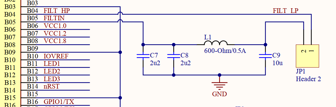
- What is the L1 in CW313. Is it just an inductor or a ferrite bead? It has the picture of the inductor but parameters like a ferrite bead.
- What is the cutoff frequency for the filter based on L1, C7, C8, C9?
- I noticed that the power traces captured by the CW has negative and positive values. What shape of the power trace in the case if the MCU is in the idle mode and most noise is filtered? Is it close to direct line where each dot on the Y-axis is about zero value?
- This question depends of the answer #3. What is ideal signal to noise ratio and how to interpret the VCC line is not noisy?
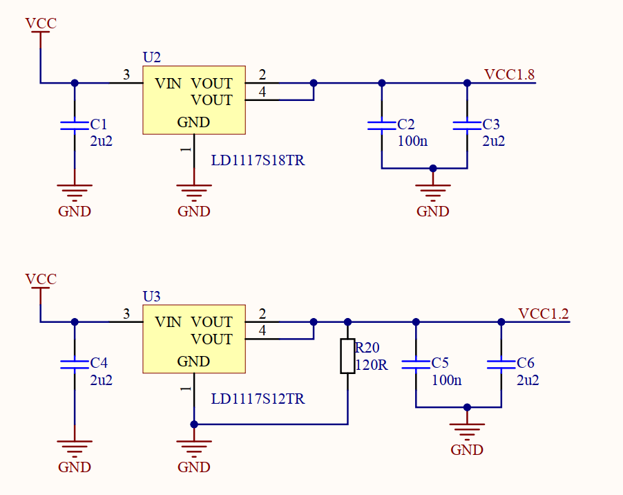
- What is the purpose of using R20 in the case of getting VCC 1.2?
Hi.
Thanks for your answers!
4. Let me rephrase/simplify my question. How to interpret the power trace quality in terms of how strong the power trace is affected by noise?
If you want an objective measurement, doing a CPA attack or something like TVLA is probably your best bet. Visually, you can do things like looking for clear patterns in the power trace or making sure that power traces line up in time, etc.
Hi. I guess, this pattern is most suitable on the well syncronized DUT!
BTW, did you ever try to use the regular 1.5V battery (directly or via voltage divider to adjust the voltage) to power the victim SoC/FPGA/microcontroller to run the side channel analysis? What are results in terms of power trace noise and attack reliability?
No, I haven’t tried that. I’d imagine that most applications would still use a regulator and there would be a large amount of bulk/decoupling capacitors on boards that would reduce the difference you’d see between that and a normal power supply.