Hello everyone,
For learning purposes I’ve been planning to run side-channel analysis, and possibly glitching, on an unknown Bluetooth + USB SoC in a consumer device from 2020. I don’t have access to a datasheet since the SoC is unknown and likely behind an NDA, so I’ve been trying to investigate it on my own before pulling the trigger on a Husky (or HuskyPlus).
I’m completely new to SCA, and still relatively new to embedded/electrical engineering in general, but I’ve been reading and preparing for a few months now.
What I’ve found so far:
-
The SoC is a 140+ ball BGA.
-
It seems to have an internal buck generating about 1.15 V. I have found no other rail (or decoupling cap) which is in the range of 0.9-1.2v.
-
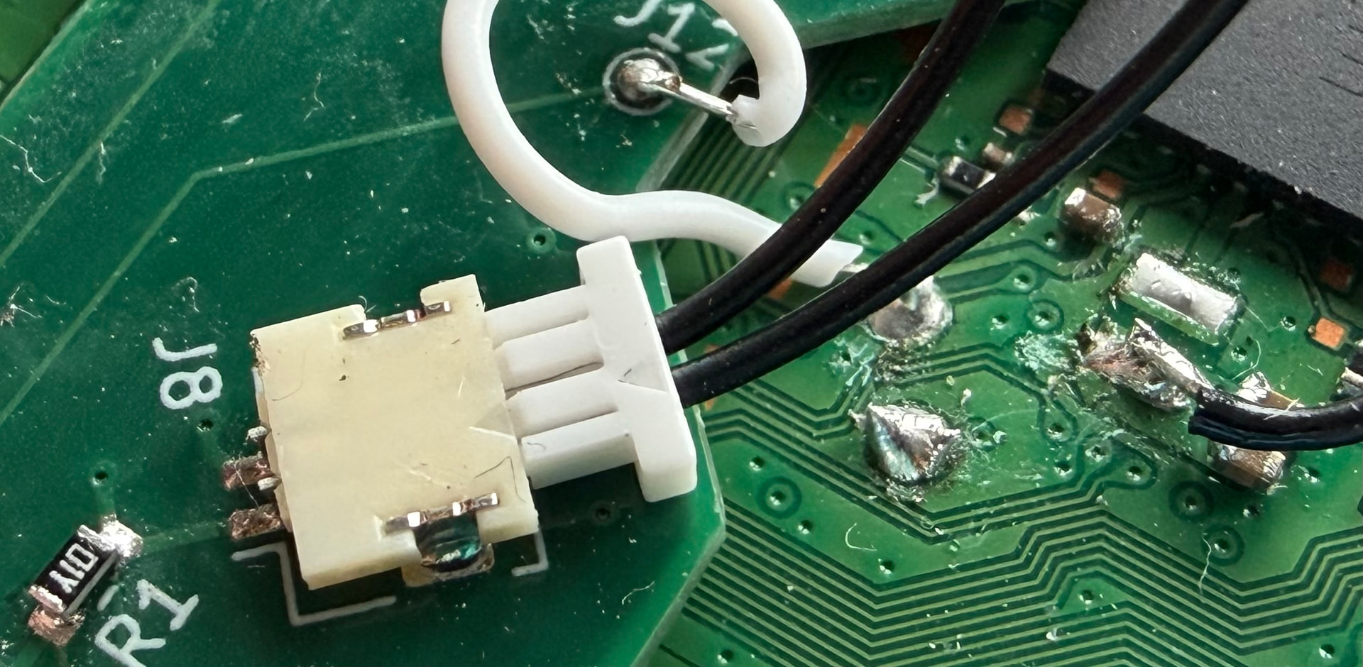
That ~1.15 V rail leaves the SoC (in a very noisy state), goes through an inductor, and then comes back into the SoC through 4 pins with nearby local decoupling.
-
My guess is that this is some kind of main low-voltage internal rail, likely digital logic and maybe more. This is my main (and only) candidate for SCA work.
-
I haven’t found any exposed clock signal for synchronous sampling, but it does have a crystal.
-
Both the crystal and the 1.15v rail are running even when the device is “sleeping” (not explicitly powered on).
I designed a small PCB to act as a frontend for this target:
-
20-pin connector for ChipWhisperer
-
SMA connectors for ShuntLow, ShuntHigh, and Crowbar
-
XTAL_OUT tap circuit that biases and digitizes the crystal output using a Schmitt trigger, then feeds it to CLOCK_IN
-
Low-noise LDO (LT3045EMSE) to supply the ~1.15 V rail externally through a shunt, so I can bypass the original buck output for a cleaner signal.
What I’ve tested so far:
-
I removed the inductor and supplied that rail externally. The device still boots and works normally.
-
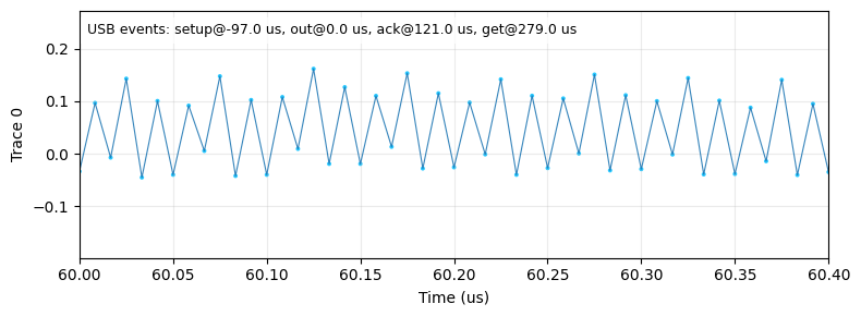
The XTAL_OUT tap works, although with my logic analyzer at 100 MS/s I only see what looks like a ~20 MHz clock with ugly duty cycle (varying between 80/20 and 60/40). I assume that is just because my sampling rate is too low to show the real waveform properly.
-
I inserted a 1.0 Ω shunt in series with the injected rail.
-
I ended up with 1.164 V on the supply side and 1.122 V on the load side during normal operation, which suggests 44 mA average current in that state.
-
The device still boots and behaves correctly with that shunt in place.
-
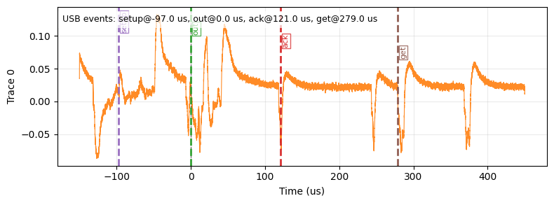
I don’t own an oscilloscope (yet), so the only analog measurements I have are from a Saleae Logic, which is obviously very limited here. But even with that, I can already see:
-
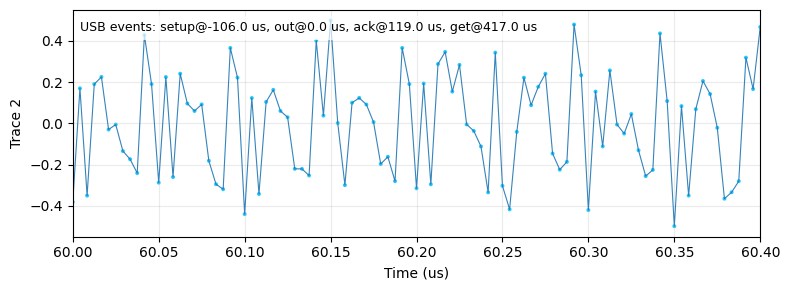
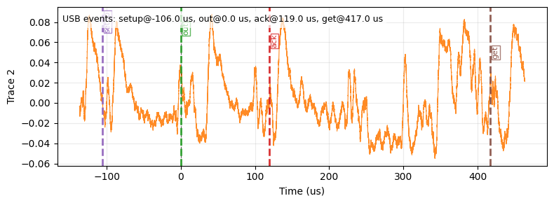
different current/activity depending on mode (USB vs Bluetooth)
-
differences between Bluetooth paired vs not paired
-
repeating pattern where it draws more current at almost exactly every 1ms - likely some repeating task?
So that makes me think I’m at least looking at a rail with real workload-dependent activity, not just some static support rail.
I’m trying to build as much confidence as possible before buying a Husky. I know starting with an unknown chip means I’m skipping quite a few steps, and I do plan to practice on known targets first, but this is my long-term goal and the main reason I started learning this.
So given all that:
-
Does this sound like a reasonable setup?
-
Does the rail work I’ve done so far sound like meaningful evidence that I’m on a useful rail for SCA?
-
An imperfect duty-cycle should be fine for the purpose of synchronous sampling, right?
-
Are there more things I could verify before pulling the trigger on a Husky?
-
Any obvious red flags in this setup?
Sorry for the long post, and thanks in advance for any feedback. I’ve mostly been learning this on my own from books (The Hardware Hacking Handbook is great!) and by bouncing ideas off LLMs, so I’d really appreciate a sanity check from people with real hands-on SCA experience.