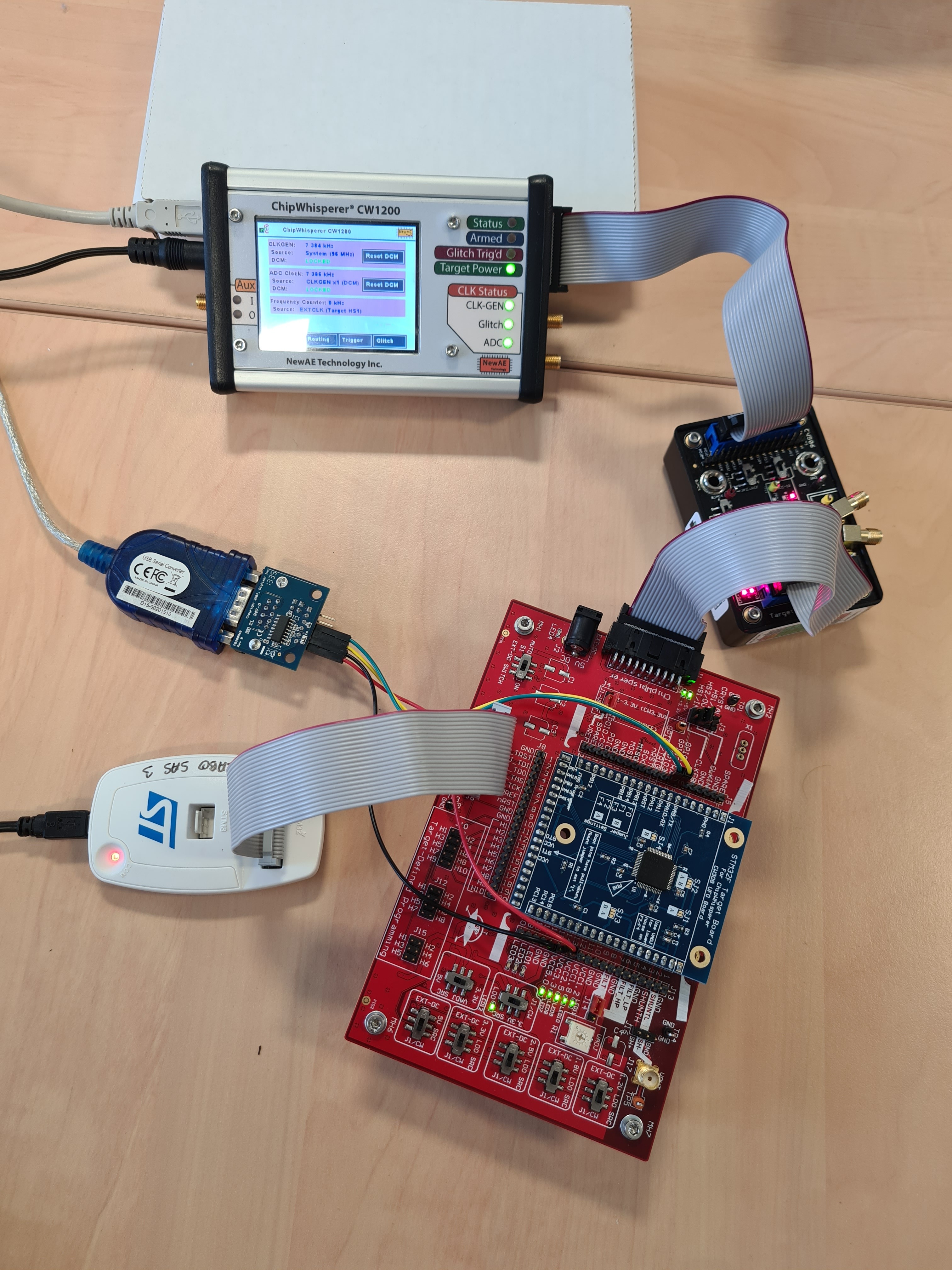
I’m using the CW308 board with a ST-Link V2 as JTAG and UART (see photo above). When I use STM32F1 I have no problem to communicate with it. But I want to use a STM32F4 and I have a problem when I try to connect to. After uploading the firmware for STM32F4 it tells that a “Read Out protection” is activated :
Loading file...
Flash Programming:
  File : C:\Users\MD264823\Desktop\Codes\M_DUMONT_et_R_VIERA\Read_Flash\src\load-CW308_STM32F4.hex
  Address : 0x08000000
Disabling read out protection...
Read out protection is activated.
It will be disabled.
Could not disable Read Out Protection!
Memory programming...
The elf loader Sector Erase function fails.
Memory-Loader error
Error occured during erase operation!
Programming Complete.
Programmed memory Checksum: 0x00000C84
On the STL-Link Soft I have the same error, and I can’t change the level of protection.
Have you ever had this problem ? Some one got any ideas how could I disable this protection ?
That read protection is designed to stop others from being able to read the code off the chip of a finished product. If you’re in RDP level 1, it should be possible to erase all the memory on the chip, but if it’s in RDP level 2, then the device is permanently unrecoverable.
That being said, it looks like that board is unfinished as its missing solder blobs on pads marked as A. If this is a home construction from one of our blank STM32F target boards, the RDP mentioned by stlink may be a red herring. If that’s the case, then you can fix it by bridging the A pads with a solder blob. If not, the microcontroller will need to be swapped out.
It worked !
Indeed, it’s a homemade board from a blank target boards. We’ve soldered STM32F1 and F4 and we noticed that on the F1 the jumper/PAD has no effect with or without solder on it. But, it seems to have its importance for F4 because, as you say, it worked after soldering A pads. Before that I also reinstall ST Link. So I couldn’t tell if it’s the soldering or the reinstallation that correct my problem. An other weirdness is that one of my three mounted STM32F4 I can’t no longer communicate with JTAG, it tells me to use SWD mode, but it’s not a big deal for now.
Thank you for your help.
These pins determine where to route power to the target, so they are quite important. I’d recommend also attaching the solder blobs on your F1 (these should be soldered to the B locations) as well.