Hello everyone,
I wanted to go a little bit deep after doing the LPC1114 tutorial and connect my actual first external target to the Nano, and the options available included the ‘blue pill’ dev board, this host a STM32F103C8T6 MCU.
Wanted to give it a try and ended in a rabbit hole, made some progress, more than expected for me to be homest, but not succesfull.
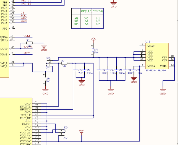
The blue pill has two 3.3v pins, one is connected to the P1 Header, is a 3x2 pin header used to boot up the bootloader, the other 3.3v pin is connected to the VDD pins of the mcu.
I made a cut of the 3.3v trace in the first pin, and added in that point a 22 ohm shunt resistor, it is placed before reaching the bootsel header, so when powering the chip from this pin the voltage need to pass across this 22ohm resisto, measuring resistence from this pin to any of the VDD input pins.on the MCU give 22.4ohm
Measuring from the other 3.3v pin or from the ‘positive pin’ of the bootsel header to the mcu VDD pins has 0 ohm, so I choose this to place the measurment pin for the nano…
I asked in discord for advice regarding removing or keeping the external oscillator, but without answer nor without knowledge I decided to remove the 8Mhz Xtal so I can attach the FPGA-HS2 pin to the OSCIN pin of the STM32.(to keep the setup as close as posible to the embeded target setup)
The connections are:
20-Pin connector - Blue Pill
2 → GND
3 → 3.3v (Closest to the bootsel header)
5 → RST
6 → OSCIN
10 → A9
12 → A10
13 → BOOT0 (middle pin at boot0 jumper)
16 → A12 / PC13 (builtin led pin)
Measure → ‘1’ (Postive pin at boot0 jumper)
GND → ‘0’ (Negative pin at boot0 jumper)
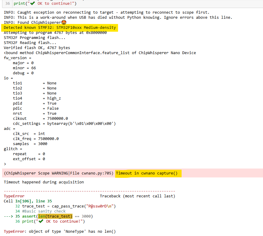
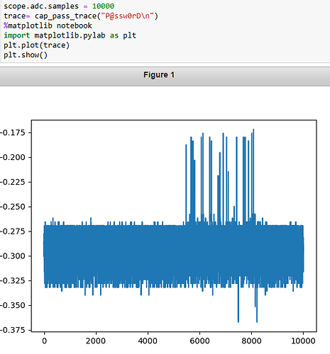
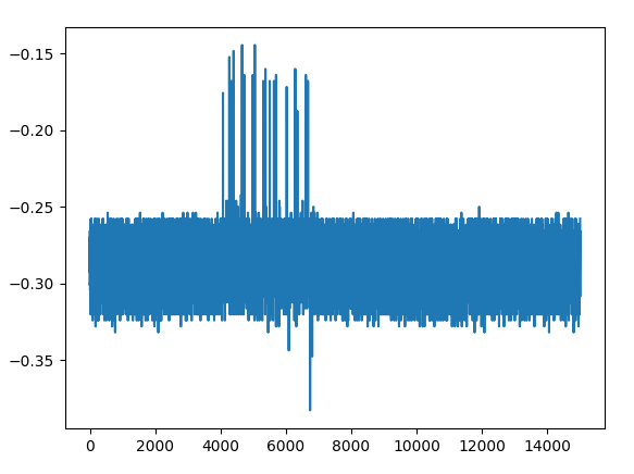
Ended being able of detect and program the target smt32 but I am unable to capture power traces properly.
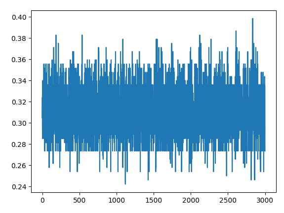
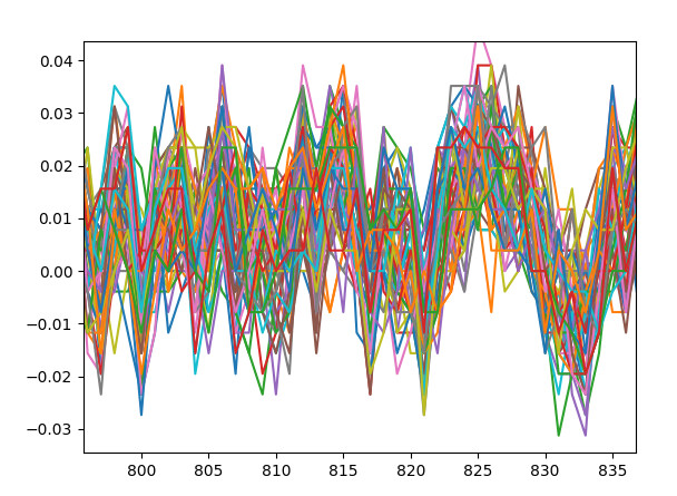
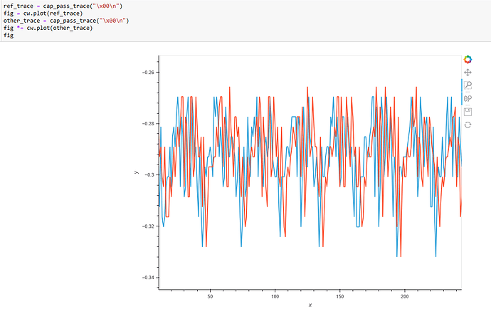
The original firmware sets up the PA12 as stm32 trigger output, but if I conect TargetIO Pin 4 to that pin i got timeout while capturing, If the trigger pin is connected to A12 I always end up with a timeout when trying to get the traces, but if I let the cable disconnected the notebook runs without errors, but I got no valid data.
To be sure triggering is working as expected, and also to have a visual confirmation, I modified the firmware to use builtin led pin (PC13) as secondary trigger source by adding this functions to hardware/victims/firmware/hal/stm32f1/stm32f1_hal.c file, note in led13_high() pin is low and in led13_low() pin is high
void led13_setup(void)
{
	__HAL_RCC_GPIOC_CLK_ENABLE();

	GPIO_InitTypeDef GpioInit;
	GpioInit.Pin       = GPIO_PIN_13;
	GpioInit.Mode      = GPIO_MODE_OUTPUT_PP;
	GpioInit.Pull      = GPIO_NOPULL;
	GpioInit.Speed     = GPIO_SPEED_FREQ_HIGH;
	HAL_GPIO_Init(GPIOC, &GpioInit);

	HAL_GPIO_WritePin(GPIOC, GPIO_PIN_13, RESET);
}

void led13_high(void)
{
	HAL_GPIO_WritePin(GPIOC, GPIO_PIN_13, RESET);
}

void led13_low(void)
{
	HAL_GPIO_WritePin(GPIOC, GPIO_PIN_13, SET);
}
Has anyone faced similar issues, can someone tellme what can be possibly wrong or what I must check to get it working?
